Cirrus Logic CS1631 User Manual
Page 38
CS1630/31
38
DS954F3
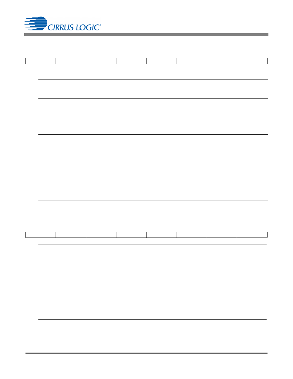
6.22 Configuration 17 (Config17)
–
Address 49
6.23 Configuration 18 (Config18)
–
Address 50
7
6
5
4
3
2
1
0
DITHER
RESYNC
T2CH2GAIN5 T2CH2GAIN4 T2CH2GAIN3 T2CH2GAIN2 T2CH2GAIN1 T2CH2GAIN0
Number
Name
Description
[7]
DITHER
Configures dither on the second stage primary side peak current threshold.
0 = Disable dither
1 = Enable dither
[6]
RESYNC
Configures resynchronization of a dual channel second stage design where
the channel synchronization circuit is not directly driven from the SYNC pin. Bit
RESYNC controls the behavior of bits EXIT_PH[3:0] and DECL_PH[3:0] (see
"Configuration 15 (Config15) – Address 47" on page 37).
0 = Disable phase resynchronization
1 = Enable phase resynchronization
[3:0]
T2CH2GAIN[5:0]
Sets T2 compensation gain T2
CH2CompGain
for channel 2 which is required
when T2 measurement compensation is enabled for flyback designs. The
value is an unsigned integer in the range of 0
T2
CH2CompGain
<63. Compen-
sated T2 time T2
Compensated
used in the second stage charge regulation loop
is given by:
where,
T2
CH2CompGain
is a decimal number the range of 0.0
T2
CH2CompGain
<4.0.
7
6
5
4
3
2
1
0
LEB3
LEB2
LEB1
LEB0
TEB3
TEB2
TEB1
TEB0
Number
Name
Description
[7:4]
LEB
[3:0]
Configures the leading-edge blanking time T
LEB
for the second stage peak
current measurement. The output of the current sense comparator which con-
trols the primary side peak current is ignored for time T
LEB
from the rising
edge of the gate drive signal.
[3:0]
TEB[3:0]
Configures the trailing-edge blanking time T
TEB
for zero-current detection. The
ZCD comparator output signal used to detect the secondary side inductor
demagnetization is blanked for time T
TEB
after the falling edge of the second
stage gate drive signal.
T2
Compensated
T2
=
Measured
T
ZCD Ri
gEdge
sin
T2
CH2CompGain
–
T2
CH2CompGain
T2CH2GAIN[5:0] 0.0625
=
T
LEB
LEB[3:0]
=
2 50ns
T
TEB
TEB[3:0]
=
2 50ns