2 output bstout sense & input iac sense, 3 boost auxiliary winding, 4 boost overvoltage protection – Cirrus Logic CS1631 User Manual
Page 15: Voltage clamp circuit, 7 voltage clamp circuit
CS1630/31
DS954F3
15
5.6.2 Output BSTOUT Sense & Input IAC
Sense
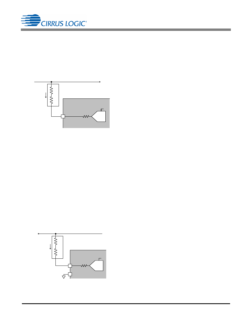
A current proportional to boost output voltage V
BST
is supplied
to the IC on pin BSTOUT and is used as a feedback control
signal (see Figure 12). The ADC is used to measure the
magnitude of current I
BSTOUT
through resistor R
BST
. The
magnitude of current I
BSTOUT
is then compared to an internal
reference current I
ref
of 133
A.
Resistor R
BST
sets the feedback current at the nominal boost
output voltage. For 230VAC line voltage applications,
resistor R
BST
is calculated as shown in Equation 4:
where,
V
BST
= nominal boost output voltage
I
ref
= internal reference current
For 120VAC line voltage applications (CS1630), nominal
boost output voltage V
BST
is 200V, and resistor R
BST
is
1.5M
. By using digital loop compensation, the voltage
feedback signal does not require an external compensation
network.
A current proportional to the AC input voltage is supplied to the
IC on pin IAC and is used by the boost control algorithm (see
Figure 13).
Resistor R
IAC
sets current I
AC
and is derived from Equation 5:
For optimal performance, resistors R
IAC
and R
BST
should use
1% tolerance or better resistors for best V
BST
voltage
accuracy.
5.6.3 Boost Auxiliary Winding
The boost auxiliary winding is used for zero-current detection
(ZCD). The voltage on the auxiliary winding is sensed through
the BSTAUX pin of the IC. It is also used to deliver startup
current during startup time (see "Startup Circuit" on page 12).
5.6.4 Boost Overvoltage Protection
The CS1630/31 supports boost overvoltage protection (BOP)
to protect the bulk capacitor C8 (see Figure 14. on page 16).
If the boost output voltage exceeds the overvoltage protection
thresholds programmed in the OTP registers a BOP fault
signal is generated. The voltage level, V
BOP(th)
, can be set
within 227V to 257V for a CS1630 and 432V to 462V for a
CS1631 (see "Configuration 53 (Config53) – Address 85" on
page 45). The control logic continuously averages the BOP
fault signal using a leaky integrator. When the output of the
leaky integrator exceeds a certain threshold, which can be set
using bits BOP_INTEG[3:0] in register Config53 (see
"Configuration 53 (Config53) – Address 85" on page 45), a
boost overvoltage fault is declared and the system stops
boosting. More information on the leaky integrator size and
sample rate is provided in section 6.23 "Configuration 18
(Config18) – Address 50" on page 38.
During a boost overvoltage protection event, the second stage
is kept enabled only if the MAX_CUR bit in register Config45
(see "Configuration 45 (Config45) – Address 77" on page 40)
is set to ‘1’ (enabled), and its dim input is railed to full scale.
This allows the second stage to quickly dissipate the stored
energy on the bulk capacitor C8, bringing down the boost
output voltage to a safe value. A visible flash on the LED might
appear, indicating that an overvoltage event has occurred.
When the boost output voltage drops to 195V (for a 120V
application), or 392V (for a 230V application), the boost stage
is enabled if bit BOP_RSTART in register Config54 (see
"Configuration 54 (Config54) – Address 86" on page 46) is set
to ‘1’, and the system returns to normal operation. If bit
BOP_RSTART is set to ‘0’, a boost overvoltage fault is latched
and the system stays in the fault mode until the input power is
recycled.
5.7 Voltage Clamp Circuit
To keep dimmers conducting and prevent them from misfiring,
a minimum power needs to be delivered from the dimmer to
the load. This power is nominally around 2W for 230V and
120V TRIAC dimmers. At low dim angles (
90°), this excess
power cannot be converted into light by the second stage due
to the dim mapping at light loads. The boost output
voltage V
BST
can rise above the safe operating voltage of the
primary-side bulk capacitor C8.
V
B S T
CS1630 /31
15k
ADC
R
B S T
I
B S TOUT
I
ref
16
BSTOUT
R8
R9
Figure 12. BSTOUT Input Pin Model
R
BST
V
BST
I
ref
--------------
400V
133
A
------------------
3M
=
=
[Eq.4]
R3
R
IA C
I
A C
IAC
V
rect
CS1630 /31
15k
ADC
R4
2
I
ref
12
Figure 13. IAC Input Pin Model
R
IAC
R
BST
=
[Eq.5]