The block diagram and description of the system, Gfg-3015 – GW Instek GFG-3015 User Manual
Page 52

p. 48 GFG-3015
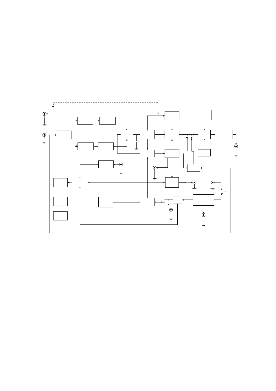
7. The Block Diagram and Description of the System
The block diagram of GFG-3015 consists of a micro processor unit (MPU), a
Voltage control Frequency (VCF), many digital to analog converters (D/A) for
corresponding block, a square and sine waveform Shaper, a modulation function
generator, a Trigger signal generator, a Frequency Counter(GFC-9701), an output
amplifier, an attenuator (ATT), and etc. The principles of generating waveforms and
Function are shown as follows:
(1) Power
Provide many kind of DC power for every block of the instrument including ± 18V,
±15V and ±5V.
(2) MPU
The Micro Processor Unit is a powerful control center of the instrument that can
control many key blocks through D/A converter including the Output waveform,
the Frequency, Amplitude, the DC offset, the Duty and the setting the parameters
of Sweep or modulation, even the Trigger function. It creates a friendly operation
environment.
In addition, it can read the output frequency through the powerful Counter
(GFC-9701) and modify the output frequency value at the real time. Therefore, it
also provides high accurate signal.
DUTYCYCLE
D/A(-)
DUTYCYCLE
D/A(+)
MOD_FUNTION
GENERATOR
10KHz~0.01Hz
DIODE
SWITCH
SINEWAVE
SHAPER
LEVEL
DETECTOR
BUFFER
AMPLIFER
AMPLIFIER
SQUARE
SHAPER
AM
FUNCTION
TTL SHAPER
MOD
TTL
TRIGGER
SIGNAL
GENERATOR
TRIGGER
PHASE
D/A
+CURRENT
SOURCE
-CURRENT
SOURCE
OFFSET
ADJUST
D/A
ATTENUATOR
MAIN
FREQUENCY
D/A
WAVE FORM
CHOICE
AM/ON
TTL OUTPUT
FREQUENEY
COUNTER
(GFC-9701)
PREAMP
AMPLIFIER
D/A
GFG-3015
GFG-3015
GFG-3015
GFG-3015
VCF INPUT
EXT
TRIGGER
MOD
INPUT
MOD
OUTPUT
COUNTER
INPUT
MAIN
OUTPUT
SYC OUTPUT
GCV OUTPUT
C
T
EXT
INT
EXT
INT
DISPLAY
UNIT
VCF unit
MPU
POWER
