Figure 4, Adsp-ts201s – Analog Devices TigerSHARC ADSP-TS201S User Manual
Page 8

Rev. C
|
Page 8 of 48
|
December 2006
ADSP-TS201S
external memory. These transfers only use handshake
mode protocol. DMA priority rotates between the four
receive channels.
• AutoDMA transfers. Two dedicated unidirectional DMA
channels transfer data received from an external bus master
to internal memory or to link port I/O. These transfers only
use slave mode protocol, and an external bus master must
initiate the transfer.
The DMA controller provides these additional features:
• Flyby transfers. Flyby operations only occur through the
external port (DMA Channel 0) and do not involve the
DSP’s core. The DMA controller acts as a conduit to trans-
fer data from an I/O device to external SDRAM memory.
During a transaction, the DSP relinquishes the external
data bus; outputs addresses and memory selects
(MSSD3–0); outputs the IORD, IOWR, IOEN, and
RD/WR strobes; and responds to ACK.
• DMA chaining. DMA chaining operations enable applica-
tions to automatically link one DMA transfer sequence to
another for continuous transmission. The sequences can
occur over different DMA channels and have different
transmission attributes.
• Two-dimensional transfers. The DMA controller can
access and transfer two-dimensional memory arrays on any
DMA transmit or receive channel. These transfers are
implemented with index, count, and modify registers for
both the X and Y dimensions.
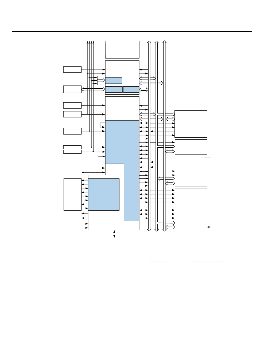
Figure 4. ADSP-TS201S Shared Memory Multiprocessing System
CLKS/REFS
ADDR31–0
DATA31–0
BR1
BR7–2,0
ADDR31–0
DATA31–0
BR0
BR7–1
BMS
CONTROL
ADSP-TS201S #0
CONTROL
ADSP-TS201S #1
ADSP-TS201S #7
ADSP-TS201S #6
ADSP-TS201S #5
ADSP-TS201S #4
ADSP-TS201S #3
ADSP-TS201S #2
RESET
RST_IN
ID2–0
CLKS/REFS
SCLK_V
REF
V
REF
SCLK
SCLKRAT2–0
000
CLOCK
REFERENCE
ADDR
DATA
HOST
PROCESSOR
INTERFACE
(OPTIONAL)
ACK
GLOBAL
MEMORY
AND
PERIPHERALS
(OPTIONAL)
OE
ADDR
DATA
CS
ADDR
DATA
BOOT
EPROM
(OPTIONAL)
RD
MS1–0
ACK
ID2–0
001
HBG
HBR
BOFF
BRST
CS
WE
WRL
C
O
N
T
R
O
L
A
D
D
R
E
S
S
D
A
T
A
C
O
N
T
R
O
L
A
D
D
R
E
S
S
D
A
T
A
SDRAM MEMORY
(OPTIONAL)
MSSD3–0
IORD
IOEN
RAS
CAS
LDQM
SDWE
SDCKE
SDA10
CS
RAS
CAS
DQM
WE
CKE
A10
ADDR
DATA
CLK
MSH
DMAR3–0
DPA
CPA
LINK
DEVICES
(2 MAX)
(OPTIONAL)
LxCLKINP/N
LxACKO
LxDATI3–0P/N
LxBCMPI
LxBCMPO
LxDATO3–0P/N
LxCLKOUTP/N
LxACKI
TMR0E
BM
CONTROLIMP1–0
LINK
IRQ3–0
FLAG3–0
LINK
RST_IN
BUSLOCK
CLOCK
DS2–0
IOWR
JTAG
POR_IN
RST_OUT
REFERENCE
LINK
DEVICES
