Test conditions, Output disable time, Adsp-ts201s – Analog Devices TigerSHARC ADSP-TS201S User Manual
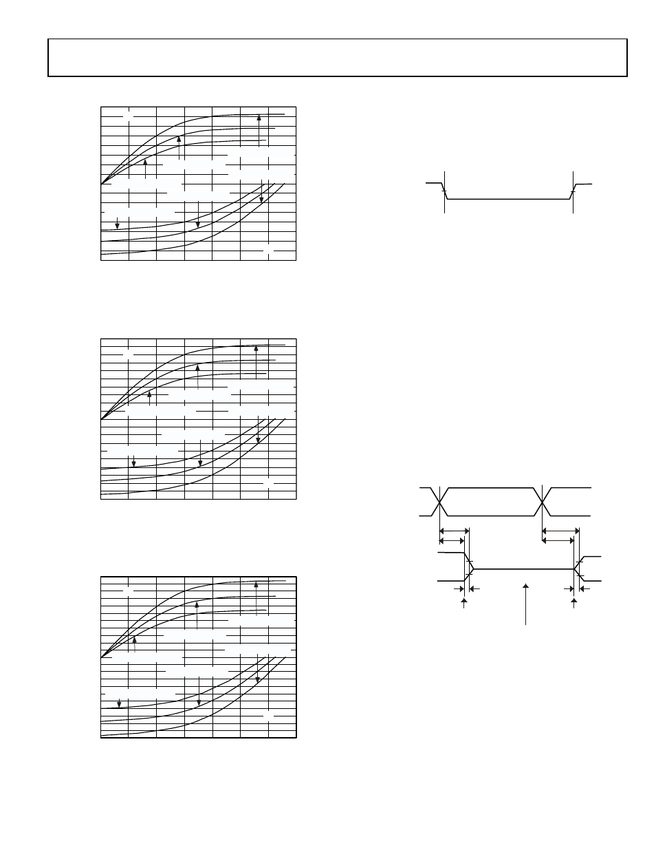
Page 37: And the load current, i, Is the difference between t, And t, As shown in figure 35 . the time t, Is calculated with test loads c, And i, And with δv equal to 0.4 v
ADSP-TS201S
Rev. C
|
Page 37 of 48
|
December 2006
TEST CONDITIONS
The ac signal specifications (timing parameters) appear in
. These include output disable time, output
enable time, and capacitive loading. The timing specifications
for the DSP apply for the voltage reference levels in
.
Output Disable Time
Output pins are considered to be disabled when they stop driv-
ing, go into a high impedance state, and start to decay from their
output high or low voltage. The time for the voltage on the bus
to decay by
ΔV is dependent on the capacitive load, C
L
and the
load current, I
L
. This decay time can be approximated by the fol-
lowing equation:
The output disable time t
DIS
is the difference between
t
MEASURED_DIS
and t
DECAY
as shown in
t
MEASURED_DIS
is the interval from when the reference signal
switches to when the output voltage decays
ΔV from the mea-
sured output high or output low voltage. t
DECAY
is calculated
with test loads C
L
and I
L
, and with
ΔV equal to 0.4 V.
Figure 31. Typical Drive Currents at Strength 5
Figure 32. Typical Drive Currents at Strength 6
Figure 33. Typical Drive Currents at Strength 7
OUTPUT PIN VOLTAGE (V)
0
2.8
0.4
0.8
1.2
1.6
2.0
2.4
O
U
T
P
U
T
P
IN
C
U
R
R
E
N
T
(m
A
)
–11
0
11
V
DD_IO
= 2.38V, +105°C
–22
–33
–44
–66
22
33
44
66
88
STRENGTH 5
V
DD_IO
= 2.5V, +25°C
V
DD_IO
= 2.63V, –40°C
I
OL
I
OH
V
DD_IO
= 2.38V, +105°C
V
DD_IO
= 2.5V, +25°C
V
DD_IO
= 2.63V, –40°C
77
55
–55
–88
–77
OUTPUT PIN VOLTAGE (V)
0
2.8
0.4
0.8
1.2
1.6
2.0
2.4
O
U
T
P
U
T
P
IN
C
U
R
R
E
N
T
(m
A
)
0
10
20
V
DD_IO
= 2.38V, +105°C
–10
–20
–30
–40
–100
30
40
50
60
100
STRENGTH 6
V
DD_IO
= 2.5V, +25°C
V
DD_IO
= 2.63V, –40°C
I
OL
I
OH
V
DD_IO
= 2.38V, +105°C
V
DD_IO
= 2.5V, +25°C
V
DD_IO
= 2.63V, –40°C
70
80
90
–50
–60
–70
–80
–90
OUTPUT PIN VOLTAGE (V)
0
2.8
0.4
0.8
1.2
1.6
2.0
2.4
O
U
T
P
U
T
P
IN
C
U
R
R
E
N
T
(m
A
)
–10
0
10
V
DD_IO
= 2.38V, +105°C
–20
–30
–40
–50
–110
20
30
40
50
110
STRENGTH 7
V
DD_IO
= 2.5V, +25°C
V
DD_IO
= 2.63V, –40°C
I
OL
I
OH
V
DD_IO
= 2.38V, +105°C
V
DD_IO
= 2.5V, +25°C
V
DD_IO
= 2.63V, –40°C
60
70
80
90
100
–60
–70
–80
–90
–100
Figure 34. Voltage Reference Levels for AC Measurements
(Except Output Enable/Disable)
Figure 35. Output Enable/Disable
INPUT
OR
OUTPUT
1.25V
1.25V
t
DECAY
C
L
V
Δ
(
) I
L
⁄
=
REFERENCE
SIGNAL
t
DIS
OUTPUT STARTS
DRIVING
V
OH (MEASURED)
–
⌬V
V
OL (MEASURED)
+
⌬V
t
MEASURED_DIS
V
OH (MEASURED)
V
OL (MEASURED)
1.65V
0.85V
HIGH IMPEDANCE STATE.
TEST CONDITIONS CAUSE THIS
VOLTAGE TO BE APPROXIMATELY 1.25V.
OUTPUT STOPS
DRIVING
t
DECAY
t
ENA
t
MEASURED_ENA
t
RAMP