Max3634, Applications information – Rainbow Electronics MAX3634 User Manual
Page 6
MAX3634
Input Stage
The LVPECL serial data input, SDI±, and burst-mode
reset input, RST±, provide 200mV
P-P
sensitivity. The
RST± input rise and fall times (20% to 80%) must not
exceed 200ps. LVPECL inputs must be DC-coupled with
external termination for correct operation with burst data
(see Maxim Application Note HFAN 1.0 for termination
configuration).
Lock Detect
After the first 12 or 13 bits of the preamble, plus 4 or 5
bits of synchronizer delay, LOCK asserts to indicate the
beginning of valid data output.
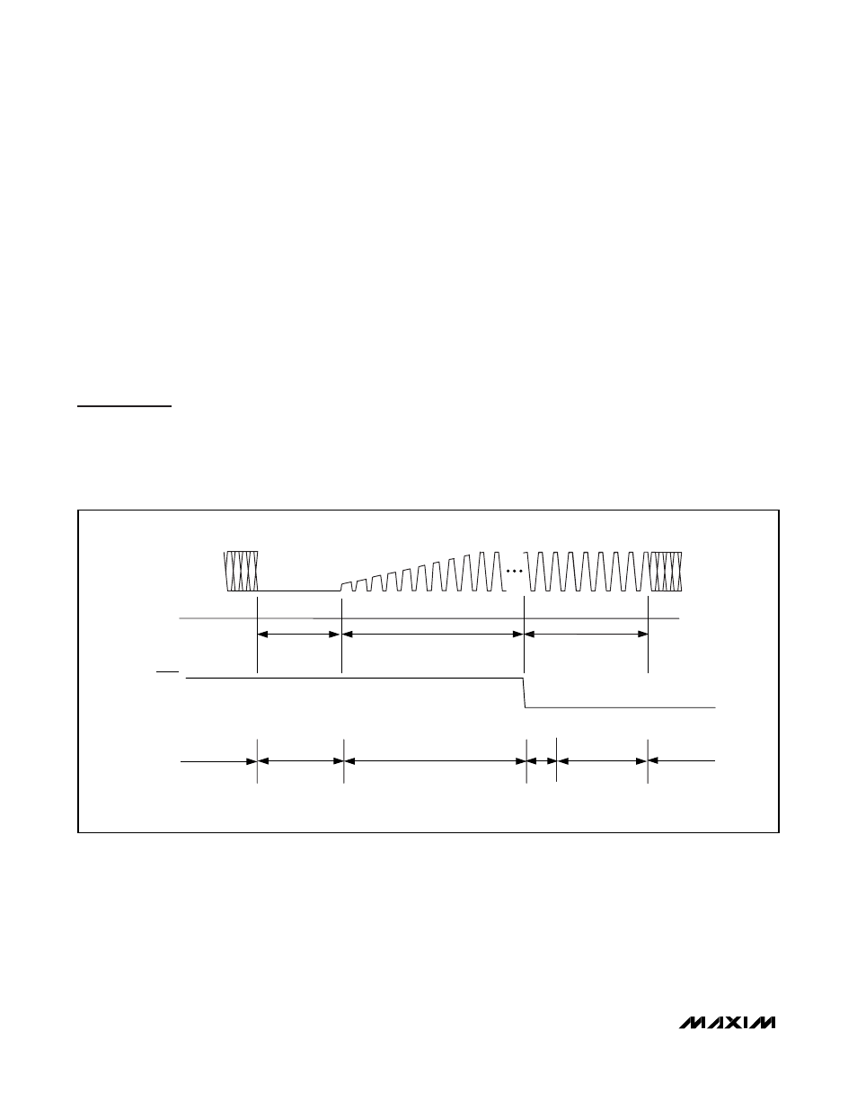
Applications Information
GPON Burst-Mode Timing
Internally, the MAX3634 requires five internal clock
cycles (8x REFCLK) to initialize itself after receiving the
rest (BRST) signal. It then uses the next 8 bits of pream-
ble (10101010) to measure the phase relationship
between the reference clock and upstream data (after
the internal logic has been reset), and 3 to 5 bits later
begins outputting data. The time interval from BRST to
the end of the preamble must be no less than 18 bits
long. If the 8 bits of preamble that it uses to measure
phase have been excessive pulse-width distortion, the
phase measurement is in error.
The active edge of the reset input (BRST) must arrive at
the MAX3634 after the TIA has finished its level recovery,
but no sooner than 18 bits prior to the end of the (repeat-
ing 10 pattern) preamble, in order to provide adequate
time for the MAX3634 to initialize, measure the phase,
and load the output pipelines. This timing is shown in
Figure 3.
622Mbps/1244Mbps Burst-Mode Clock Phase
Aligner for GPON OLT Applications
6
_______________________________________________________________________________________
DATA INPUT
TO MAX3634
RESET
T
DSR
: BURST-TO-BURST SEPARATION TIME
T
LR
: TIA/LA LEVEL RECOVERY TIME
T
CR
: CPA RESET AND ACQUISITION TIME,
≥ 19 BITS
T
DSR
DATA VALID
GUARD TIME
TIA/LA ACQUISITION
CPA RESET
(5 BITS)
CPA ACQUISITION
(12 OR 13 BITS)
OUTPUT DATA
VALID
T
LR
T
CR
Figure 3. Clock Phase Aligner Operation Timing Diagram