Pin description, At73c501 single-ended adc – Rainbow Electronics AT73C502 User Manual
Page 3
AT73C500
3
Pin Description
AT73C501 Single-ended ADC
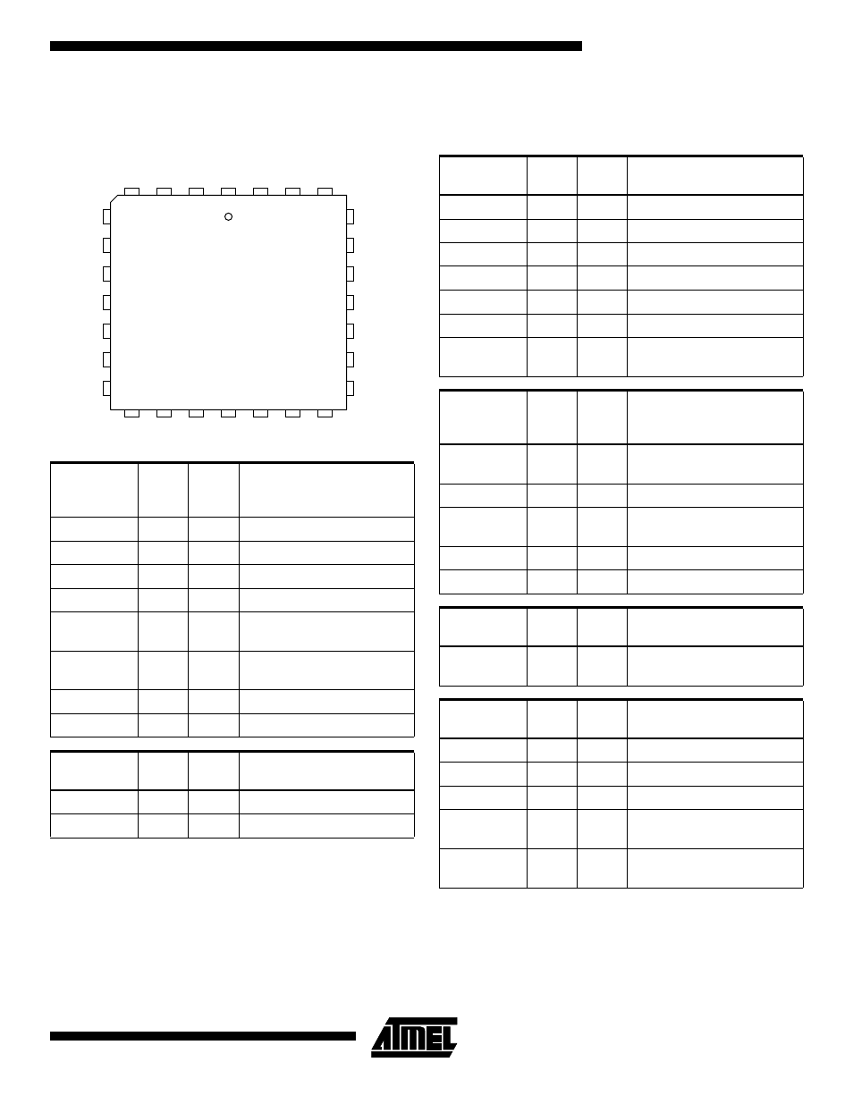
Figure 3. PLCC-28 package pin layout
Power
Supply
Pins
Pin
I/O
Description
VDDA
13
PWR
Analog Supply, Positive, +5V
VSSA
12
PWR
Analog Supply, Negative, 0V
VDA
21
PWR
Analog Supply, Positive, +5V
VSA
20
PWR
Analog Supply, Negative, 0V
AGND
9
PWR
Analog Ground Reference
Input
VREF 11
PWR
Reference Voltage
Output/Input
VCC
7
PWR
Digital Supply, Positive, +5V
VGND
23
PWR
Digital Supply, Negative, 0V
Crystal Osc
Signals
Pin
I/O
Description
XI
3
I
Crystal Oscillator Input
XO
4
O
Crystal Oscillator Output
RESET
DATA
FSR
ACK
CLKR
CLK
XI
XO
25
26
27
28
1
2
N/C
3
4
24
VGND
23
PD
22
VDA
21
VSA
20
AIN5
19
VSSA VDDA AIN2
AIN4
AIN6
AIN1
AIN3
18
17
16
15
14
13
12
BGD
CS
VCC
PFAI
AGN
VCIN
VREF
5
6
7
8
9
10
11
Analog
Signals
Pin
I/O
Description
AIN1
17
I
Current, Channel 1
AIN2
14
I
Voltage, Channel 1
AIN3
18
I
Current, Channel 2
AIN4
15
I
Voltage, Channel 2
AIN5
19
I
Current, Channel 3
AIN6
16
I
Voltage, Channel 3
VCIN
10
I
Input to Voltage Monitoring
Block
Digital
Control
Signals
Pin
I/O
Description
BGD
5
I
By-pass Control
for Reference Voltage
CS
6
I
Chip Select Input
PD
22
I
Power Down Control
for A/D Modulators
N/C
24
I
Connect to VGND
RESET
25
I
Reset Input, Active High
Status
Flags
Pin
I/O
Description
PFAIL
8
O
Output of Voltage Monitoring
Block
Output Bus
Signals
Pin
I/O
Description
CLK
2
O
Master Clock Output
CLKR
1
O
Serial Bus Clock Output
DATA
26
O
Serial Data Output
FSR
27
O
Output Sample Frame
Signal
ACK
28
O
Data Ready Acknowledge
Output