Write operations, Cs si (input) – Rainbow Electronics AT45DB021E User Manual
Page 52
52
AT45DB021E [PRELIMINARY DATASHEET]
8789B–DFLASH–11/2012
23.
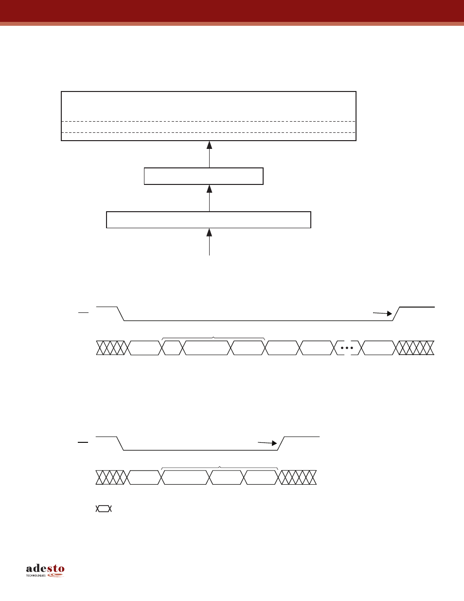
Write Operations
The following block diagram and waveforms illustrate the various write sequences available.
Figure 23-1. Block Diagram
Figure 23-2. Buffer Write
Figure 23-3. Buffer to Main Memory Page Program
Flash Memory Array
I/O Interface
SI
Buffer To
Main Memory
Page Program
Buffer
Write
Page (256/264 bytes)
Buffer (256/264 bytes)
CS
SI (Input)
CMD
X
X···X, BFA8
BFA7-0
n
n + 1
Last Byte
Completes Writing into Selected Buffer
Binary Page Size
16 Dummy Bits + BFA7-BFA0
CS
SI (Input)
CMD
PA9-7
PA6-0, X
XXXX XXX
Starts Self-timed Erase/Program Operation
Binary Page Size
A17-A8 + 8 Dummy Bits
n = 1st byte read
n+1 = 2nd byte read
Each transition represents eight bits
See also other documents in the category Rainbow Electronics Storage:
- W27E010 (14 pages)
- W27L520 (16 pages)
- W29EE512 (21 pages)
- W27E512 (16 pages)
- W24100 (11 pages)
- W27E040 (15 pages)
- W25Q32 (60 pages)
- W49L102 (21 pages)
- W29C040 (20 pages)
- W29EE011 (20 pages)
- W49F020 (21 pages)
- W2465 (10 pages)
- W24256 (10 pages)
- W982516CH (43 pages)
- MAX16014 (12 pages)
- W24512A (10 pages)
- W27E020 (14 pages)
- W29C020C (21 pages)
- W25X64 (47 pages)
- W24257 (11 pages)
- W24L257 (10 pages)
- W9864G2GH (48 pages)
- W24L11 (11 pages)
- W27L010 (14 pages)
- W27E520 (16 pages)
- W27LE520 (16 pages)
- W9825G6CH (43 pages)
- W49F002U (23 pages)
- W9864G6GB (47 pages)
- AT45DB011B (32 pages)
- AT45DB642 (71 pages)
- AT45DB642 (37 pages)
- AT45DB161D (51 pages)
- AT27LV040A (12 pages)
- AT29LV010A (15 pages)
- HT24LC08 (11 pages)
- AT29C257 (12 pages)
- AT45DB161B (32 pages)
- AT27C1024 (12 pages)
- AT28BV256 (12 pages)
- AT28C040 (12 pages)
- DS1258Y_AB (9 pages)
- AT28BV64B (12 pages)
- AT27C512R (12 pages)
- DS1220AB_AD (9 pages)