Memory array – Rainbow Electronics AT45DB021E User Manual
Page 5
5
AT45DB021E [PRELIMINARY DATASHEET]
8789B–DFLASH–11/2012
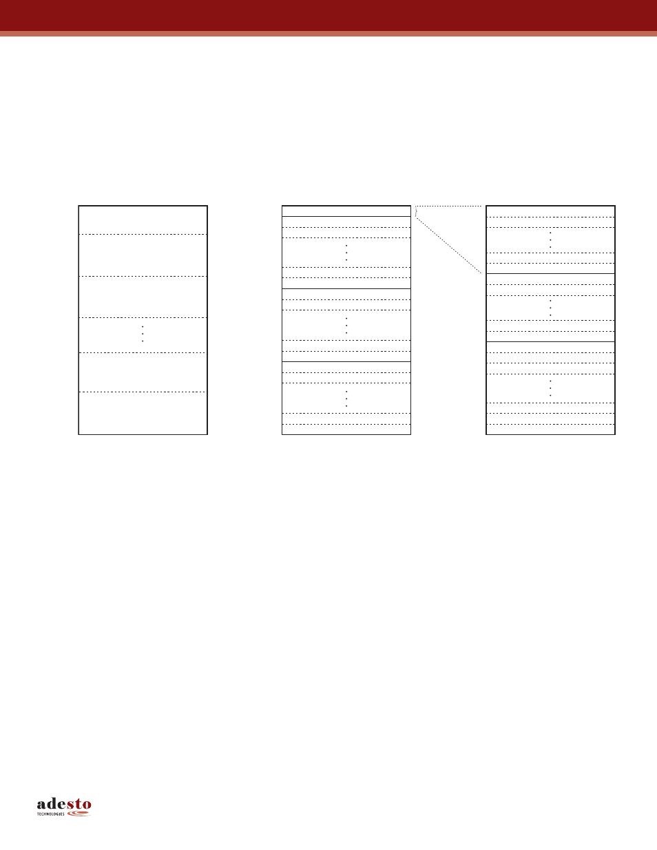
3.
Memory Array
To provide optimal flexibility, the AT45DB021E memory array is divided into three levels of granularity comprising of
sectors, blocks, and pages.
Figure 3-1, Memory Architecture Diagram
illustrates the breakdown of each level and details
the number of pages per sector and block. Program operations to the DataFlash can be done at the full page level or at
the byte level (a variable number of bytes). The erase operations can be performed at the chip, sector, block, or page
level.
Figure 3-1. Memory Architecture Diagram
Sector 0a = 8 pages
2,048/2,112 bytes
Sector 0b = 120 pages
30,720/31,680 bytes
Block = 2,048/2,112 bytes
8 Pages
Sector 0a
Sector 0b
Page = 256/264 bytes
Page 0
Page 1
Page 6
Page 7
Page 8
Page 9
Page 1,022
Page 1,023
Block 0
Page 14
Page 15
Page 16
Page 17
Page 18
Block 1
Sector Architecture
Block Architecture
Page Architecture
Block 0
Block 1
Block 14
Block 15
Block 16
Block 17
Block 46
Block 47
Block 30
Block 31
Block 32
Block 33
Sector 1
Sector 2
Sector 7 = 128 pages
32,768/33,792 bytes
Block 2
Sector 1 = 128 pages
32,768/33,792 bytes
Sector 6 = 128 pages
32,768/33,792 bytes