Buffer and page size configuration – Rainbow Electronics AT45DB021E User Manual
Page 33
33
AT45DB021E [PRELIMINARY DATASHEET]
8789B–DFLASH–11/2012
11.
Buffer and Page Size Configuration
The memory array of DataFlash devices is actually larger than other Serial Flash devices in that extra user-accessible
bytes are provided in each page of the memory array. For the AT45DB021E, there are an extra eight bytes of memory in
each page for a total of an extra 8KB (64-Kbits) of user-accessible memory.
Some applications, however, may not want to take advantage of this extra memory and instead architect their software to
operate on a “power of 2” binary, logical addressing scheme. To allow this, the DataFlash can be configured so that the
Buffer and page sizes are 256 bytes instead of the standard 264 bytes. In addition, the configuration of the Buffer and
page sizes is reversible and can be changed from 264 bytes to 256 bytes or from 256 bytes to 264 bytes. The configured
setting is stored in an internal nonvolatile register so that the Buffer and page size configuration is not affected by power
cycles. The nonvolatile register has a limit of 10,000 erase/program cycles; therefore, care should be taken to not switch
between the size options more than 10,000 times.
Devices are initially shipped from Adesto with the Buffer and page sizes set to 264 bytes. Devices can be ordered from
Adesto pre-configured for the “power of 2” binary size of 256 bytes. For details, see
Section 27., "Ordering Information"
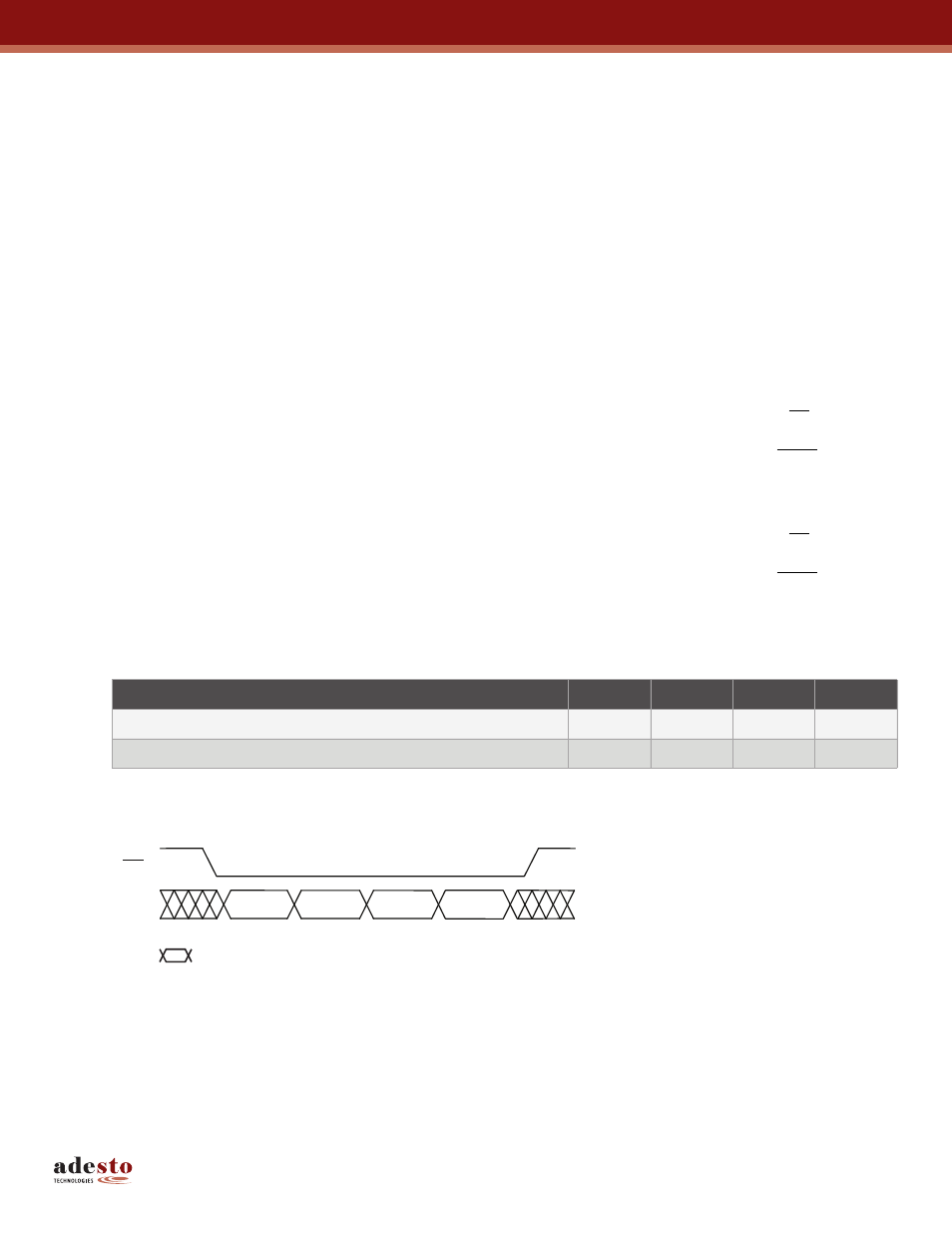
To configure the device for “power of 2” binary page size (256 bytes), a 4-byte opcode sequence of 3Dh, 2Ah, 80h, and
A6h must be clocked into the device. After the last bit of the opcode sequence has been clocked in, the CS pin must be
deasserted to initiate the internally self-timed configuration process and nonvolatile register program cycle. The
programming of the nonvolatile register should take place in a time of t
EP
, during which time, the RDY/BUSY
bit in the
Status Register will indicate that the device is busy. The device does not need to be power cycled after the completion of
the configuration process and register program cycle in order for the Buffer and page size to be configured to 256 bytes.
To configure the device for standard DataFlash page size (264 bytes), a 4-byte opcode sequence of 3Dh, 2Ah, 80h, and
A7h must be clocked into the device. After the last bit of the opcode sequence has been clocked in, the CS pin must be
deasserted to initial the internally self-timed configuration process and nonvolatile register program cycle. The
programming of the nonvolatile register should take place in a time of t
EP
, during which time, the RDY/BUSY
bit in the
Status Register will indicate that the device is busy. The device does not need to be power cycled after the completion of
the configuration process and register program cycle in order for the Buffer and page size to be configured to 264 bytes.
Table 11-1. Buffer and Page Size Configuration Commands
Figure 11-1. Buffer and Page Size Configuration
Command
Byte 1
Byte 2
Byte 3
Byte 4
“Power of 2” binary page size (256 bytes)
3Dh
2Ah
80h
A6h
DataFlash page size (264 bytes)
3Dh
2Ah
80h
A7h
CS
SI
3Dh
2Ah
80h
Opcode
Byte 4
Each transition represents eight bits