Rainbow Electronics DS1852 User Manual
Page 13
DS1852
13 of 25
MEMORY MAP
Memory access to the DS1852 is through the 2-wire interface. See the 2-WIRE OPERATION section.
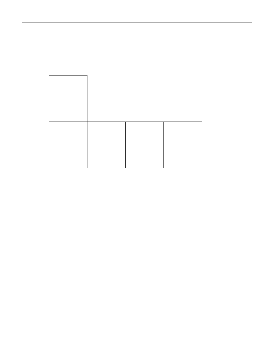
The memory within the DS1852 is organized into multiple tables. The lower 128 bytes of memory are
common to all tables, the upper 128 bytes are addressed according to the table select byte at 7Fh. Valid
values of the table address byte are 00h to 03h, to access Tables 00h through 03h.
*For permission details of this memory block refer to following table.
The following tables detail the memory contents. Where descriptions are underlined an expanded table
indicates the function of individual bits within the byte. The reserved memory locations should not be
used even though R/W access may be possible.
Not all memory is EEPROM; RAM cells are shaded within the tables, and denoted beneath.
Tables 00h –
03h
Lower
128 bytes
R- All
W - Level 2*
80h
Table 00h
Upper
128 Bytes
No Physical
Memory
Table 03h
Upper
128 Bytes
R/W - Level 2
Table 02h
Upper
128 Bytes
R/W - Level 2
Table 01h
Upper
128 Bytes
R/W - Level 1
FF
80h
80h
80h
FF
FF
FF
00h
7Fh