Alu – arithmetic logic unit, Programmable flash program memory, Sram data memory – Rainbow Electronics AT90C8534 User Manual
Page 8
AT90C8534
8
ALU – Arithmetic Logic Unit
The high-performance AVR ALU operates in direct connection with all the 32 general-purpose working registers. Within a
single clock cycle, ALU operations between registers in the register file are executed. The ALU operations are divided into
three main categories: arithmetic, logical and bit functions.
Programmable Flash Program Memory
The AT90C8534 contains 8K bytes of on-chip programmable Flash memory for program storage. Since all instructions are
16- or 32-bit words, the Flash is organized as 4K x 16. The Flash memory has an endurance of at least 1000 write/erase
cycles. The AT90C8534 program counter (PC) is 12 bits wide, thus addressing the 4096 program memory addresses.
Constant tables must be allocated within the address 0 - 4K (see the LPM – Load Program Memory instruction description).
See page 9 for the different program memory addressing modes.
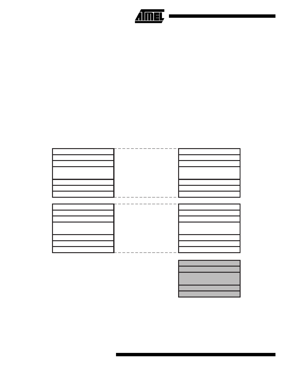
SRAM Data Memory
The following figure shows how the AT90C8534 SRAM memory is organized.
Figure 8. SRAM Organization
The lower 352 data memory locations address the register file, the I/O memory and the internal data SRAM. The first
96 locations address the register file + I/O memory, and the next 256 locations address the internal data SRAM.
The five different addressing modes for the data memory cover: Direct, Indirect with Displacement, Indirect, Indirect with
Pre-decrement and Indirect with Post-increment. In the register file, registers R26 to R31 feature the indirect addressing
pointer registers.
The direct addressing reaches the entire data space.
Register File
R0
R1
R2
R29
R30
R31
I/O Registers
$00
$01
$02
...
$3D
$3E
$3F
...
$0000
$0001
$0002
$001D
$001E
$001F
$0020
$0021
$0022
...
$005D
$005E
$005F
...
Data Address Space
$0060
$0061
$015E
$015F
...
Internal SRAM