Rainbow Electronics AT90C8534 User Manual
Page 15
AT90C8534
15
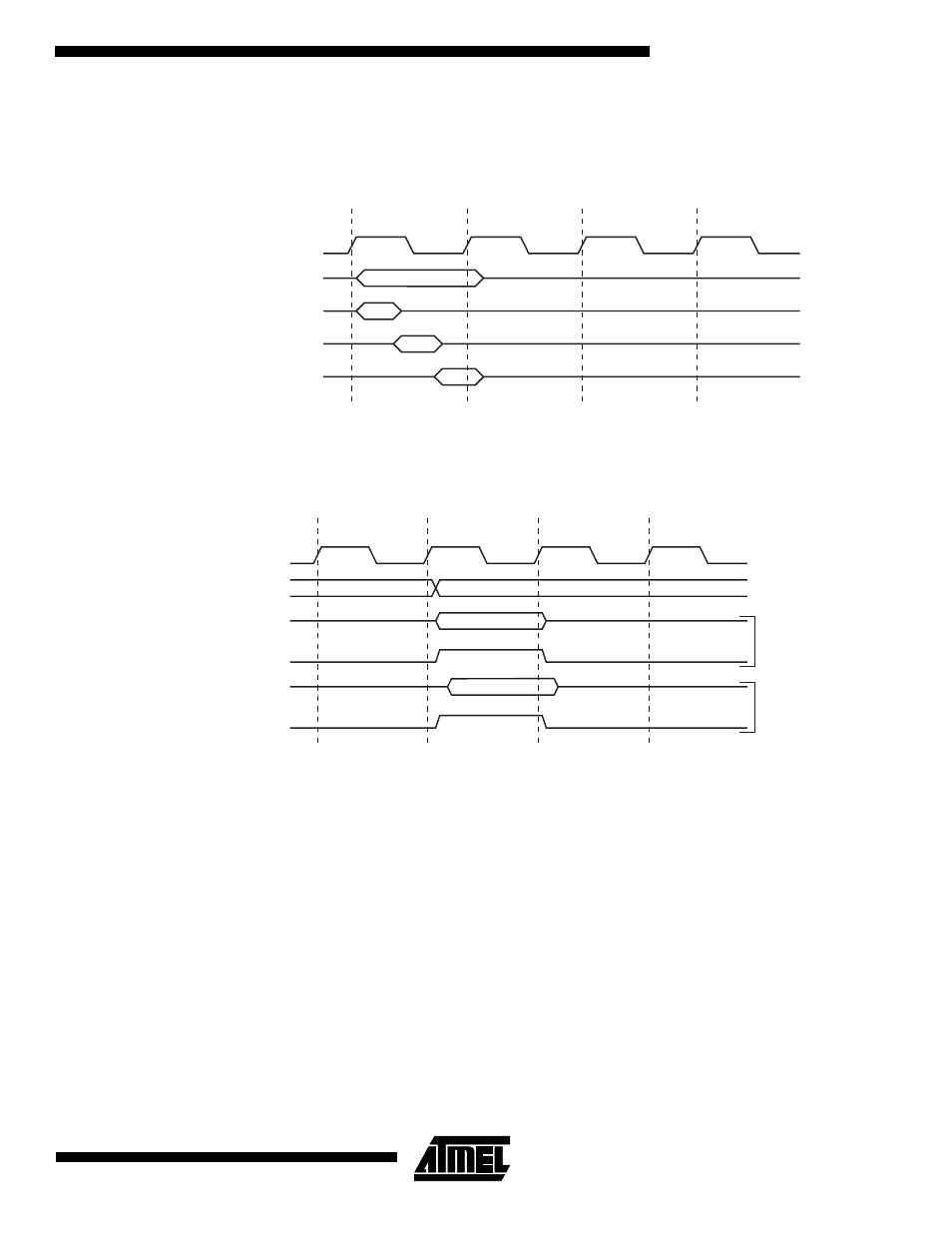
Figure 21 shows the internal timing concept for the register file. In a single clock cycle an ALU operation using two register
operands is executed and the result is stored back to the destination register.
Figure 21. Single Cycle ALU Operation
The internal data SRAM access is performed in two System Clock cycles as described in Figure 22.
Figure 22. On-Chip Data SRAM Access Cycles
System Clock Ø
Total Execution Time
Register Operands Fetch
ALU Operation Execute
Result Write Back
T1
T2
T3
T4
System Clock Ø
WR
RD
Data
Data
Address
Address
T1
T2
T3
T4
Prev. Address
Read
Wr
ite
See also other documents in the category Rainbow Electronics Sensors:
- MAX5151 (16 pages)
- MAXQ3108 (64 pages)
- MAX5661 (39 pages)
- MAX6691 (7 pages)
- MAX5362 (12 pages)
- ADC10158 (26 pages)
- MAX8922L (14 pages)
- MAX8596Z (8 pages)
- MAX7491 (18 pages)
- MAX15040 (15 pages)
- MAX5177 (16 pages)
- ADC08138 (22 pages)
- MAX5961 (42 pages)
- T89C51RD2 (86 pages)
- MAX16055 (9 pages)
- MAX6659 (17 pages)
- ADC0820 (20 pages)
- MAX6678 (19 pages)
- MAX8884Z (15 pages)
- MAX16915 (9 pages)
- MAX8620 (18 pages)
- MAX5144 (12 pages)
- MAX6670 (8 pages)
- MAX8760 (39 pages)
- W78C32C (14 pages)
- MX7533 (8 pages)
- MAX8727 (13 pages)
- MAX9053 (15 pages)
- W78C54 (16 pages)
- MAX8614B (15 pages)
- W90N740 (219 pages)
- MAX6626 (13 pages)
- ADC10738 (30 pages)
- MAX17000 (31 pages)
- MAX5051 (21 pages)
- MAXQ1004 (18 pages)
- MAX6871 (51 pages)
- MX7847 (12 pages)
- MAX6608 (6 pages)
- MAX17083 (15 pages)
- MAX6641 (17 pages)
- MAX5251 (16 pages)
- MAX6338 (8 pages)
- MAX6690 (16 pages)
- MAX8668 (18 pages)