Rainbow Electronics AT90C8534 User Manual
Page 5
AT90C8534
5
The I/O memory space contains 64 addresses for CPU peripheral functions such as Control Registers, Timer/Counters,
A/D converters and other I/O functions. The I/O memory can be accessed directly or as the Data Space locations
following those of the register file, $20 - $5F.
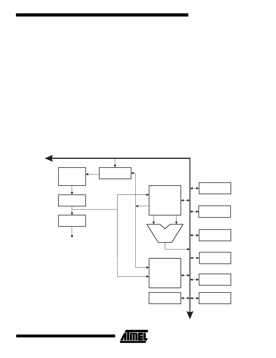
The AVR uses a Harvard architecture concept – with separate memories and buses for program and data. The program
memory is executed with a single-level pipelining. While one instruction is being executed, the next instruction is
pre-fetched from the program memory. This concept enables instructions to be executed in every clock cycle. The program
memory is programmable Flash memory.
With the relative jump and call instructions, the whole 4K word (8K bytes) address space is directly accessed. Most AVR
instructions have a single 16-bit word format. Every program memory address contains a 16- or 32-bit instruction.
During interrupts and subroutine calls, the return address program counter (PC) is stored on the stack. The stack is effec-
tively allocated in the general data SRAM and, consequently, the stack size is only limited by the total SRAM size and the
usage of the SRAM. All user programs must initialize the stack pointer (SP) in the reset routine (before subroutines or
interrupts are executed). The 9-bit stack pointer is read/write accessible in the I/O space.
The 256 bytes data SRAM can be easily accessed through the five different addressing modes supported in the AVR
architecture.
The memory spaces in the AVR architecture are all linear and regular memory maps.
Figure 4. The AT90C8534 AVR RISC Architecture
4K X 16
Program
Memory
Instruction
Register
Instruction
Decoder
Program
Counter
Control Lines
32 x 8
General
Purpose
Registrers
ALU
Status
and Control
Interrupt
Unit
8-bit
Timer/Counter
Analog to Digital
Converter
7
Output Lines
512 x 8
EEPROM
Data Bus 8-bit
AVR AT90C8534 Architecture
256 x 8
Data
SRAM
Direct Addressing
Indirect Addressing
16-bit
Timer/Counter