Timer/counter0 control register – tccr0 – Rainbow Electronics AT90C8534 User Manual
Page 25
AT90C8534
25
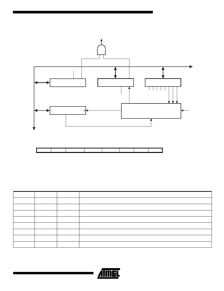
Figure 27. Timer/Counter0 Block Diagram
Timer/Counter0 Control Register – TCCR0
•
Bits 7..3 – Res: Reserved Bits
These bits are reserved bits in the AT90C8534 and always read zero.
•
Bits 2, 1, 0 – CS02, CS01, CS00: Clock Select0, Bits 2, 1 and 0
The Clock Select0 bits 2, 1 and 0 define the prescaling source of Timer/Counter0.
The Stop condition provides a Timer Enable/Disable function. The prescaled CK modes are scaled directly from the CK
oscillator clock.
Bit
7
6
5
4
3
2
1
0
$33 ($53)
–
–
–
–
–
CS02
CS01
CS00
TCCR0
Read/Write
R
R
R
R
R
R/W
R/W
R/W
Initial value
0
0
0
0
0
0
0
0
Table 4. Clock 0 Prescale Select
CS02
CS01
CS00
Description
0
0
0
Stop, Timer/Counter0 is stopped.
0
0
1
CK
0
1
0
CK/8
0
1
1
CK/64
1
0
0
CK/256
1
0
1
CK/1024
1
1
0
Reserved
1
1
1
Reserved
8-BIT DA
T
A
BUS
T/C0 CONTROL
REGISTER (TCCR0)
TIMER/COUNTER0
(TCNT0)
0
7
T/C CLK SOURCE
CONTROL
LOGIC
CS02
CS01
CS00
CK
T/C0 OVER-
FLOW IRQ
TIMER INT. MASK
REGISTER (TIMSK)
TOIE0
TOIE1
TIMER INT. FLAG
REGISTER (TIFR)
TOV0
TOV1
- MAX5151 (16 pages)
- MAXQ3108 (64 pages)
- MAX5661 (39 pages)
- MAX6691 (7 pages)
- MAX5362 (12 pages)
- ADC10158 (26 pages)
- MAX8922L (14 pages)
- MAX8596Z (8 pages)
- MAX7491 (18 pages)
- MAX15040 (15 pages)
- MAX5177 (16 pages)
- ADC08138 (22 pages)
- MAX5961 (42 pages)
- T89C51RD2 (86 pages)
- MAX16055 (9 pages)
- MAX6659 (17 pages)
- ADC0820 (20 pages)
- MAX6678 (19 pages)
- MAX8884Z (15 pages)
- MAX16915 (9 pages)
- MAX8620 (18 pages)
- MAX5144 (12 pages)
- MAX6670 (8 pages)
- MAX8760 (39 pages)
- W78C32C (14 pages)
- MX7533 (8 pages)
- MAX8727 (13 pages)
- MAX9053 (15 pages)
- W78C54 (16 pages)
- MAX8614B (15 pages)
- W90N740 (219 pages)
- MAX6626 (13 pages)
- ADC10738 (30 pages)
- MAX17000 (31 pages)
- MAX5051 (21 pages)
- MAXQ1004 (18 pages)
- MAX6871 (51 pages)
- MX7847 (12 pages)
- MAX6608 (6 pages)
- MAX17083 (15 pages)
- MAX6641 (17 pages)
- MAX5251 (16 pages)
- MAX6338 (8 pages)
- MAX6690 (16 pages)
- MAX8668 (18 pages)