Prescaling – Rainbow Electronics AT90C8534 User Manual
Page 31
AT90C8534
31
A conversion is started by writing a logical “1” to the ADC Start Conversion bit, ADSC. This bit stays high as long as the
conversion is in progress and will be set to zero by hardware when the conversion is completed. If a different data channel
is selected while a conversion is in progress, the ADC will finish the current conversion before performing the channel
change.
As the ADC generates a 10-bit result, two data registers, ADCH and ADCL, must be read to get the result when the conver-
sion is complete. Special data protection logic is used to ensure that the contents of the data registers belong to the same
conversion when they are read. This mechanism works as follows:
When reading data, ADCL must be read first. Once ADCL is read, ADC access to data registers is blocked. This means
that if ADCL has been read, and a conversion completes before ADCH is read, none of the registers are updated and the
result from the conversion is lost. When ADCH is read, ADC access to the ADCH and ADCL registers is re-enabled.
The ADC has its own interrupt, ADIF, which can be triggered when a conversion completes. When ADC access to the data
registers is prohibited between reading of ADCH and ADCL, the interrupt will trigger even if the result gets lost.
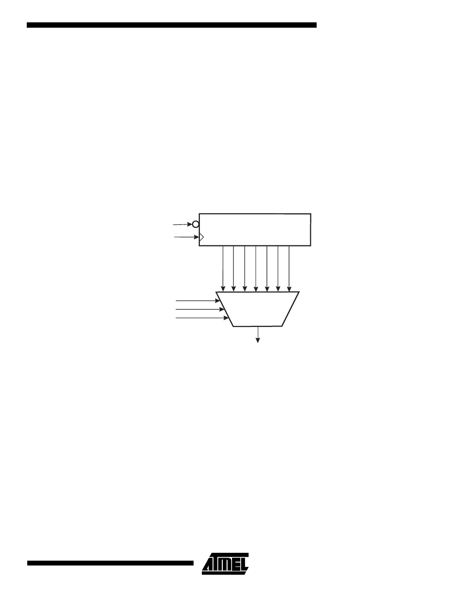
Prescaling
Figure 30. ADC Prescaler
The ADC contains a prescaler, which divides the system clock to an acceptable ADC clock frequency. The ADC accepts
input clock frequencies in the range of 80 - 170 kHz.
The ADPS0 - ADPS2 bits in ADCSR are used to generate a proper ADC clock input frequency from any XTAL frequency
above 160 kHz. The prescaler starts counting from the moment the ADC is switched on by setting the ADEN bit in ADCSR.
The prescaler keeps running for as long as the ADEN bit is set, and is continuously reset when ADEN is low.
When initiating a conversion by setting the ADSC bit in ADCSR, the conversion starts at the following rising edge of the
ADC clock cycle. The actual sample-and-hold takes place 1.5 ADC clock cycles after the start of the conversion. The result
is ready and written to the ADC Result Register after 13 cycles. In Single Conversion Mode, the ADC needs one more
clock cycle before a new conversion can be started (see Figure 32). If ADSC is set high in this period, the ADC will start the
new conversion immediately. In Free Run Mode, a new conversion will be started immediately after the result is written to
the ADC Result Register. Using Free Run Mode and an ADC clock frequency of 170 kHz gives the lowest conversion time,
76 µs, equivalent to 13 kSPS. For a summary of conversion times, see Table 6.
7-BIT ADC PRESCALER
ADC CLOCK SOURCE
CK
ADPS0
ADPS1
ADPS2
CK/128
CK/2
CK/4
CK/8
CK/16
CK/32
CK/64
Reset
ADEN