Rainbow Electronics TS81102G0 User Manual
Page 30
30
TS81102G0
2105C–BDC–11/03
Applying the
TS81102G0
DMUX
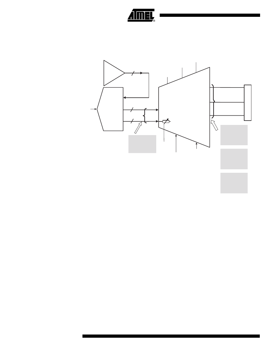
The TSEV81102G0 DMUX evaluation board is designed to be connected with the
TSEV8388G and TSEV83102G0 ADC evaluation boards.
Figure 25.
TSEV81102G0 DMUX Evaluation Boards
Please refer to the "ADC and DMUX Application Note" for more information.
Delay
adjust
control
CLOCK
BUFFER
s-e or diff.
(2 GHz)
FS
Analog
Input
ADC
Clkln
Data
Bus
Data
Ready
(1 GHz)
8b/10b diff.
ECL
Rload = 50
Ω
Vih = -1.0V
Vil = -1.4V
DEMUX
(125 MHz)
8x8b/10b single
(DC)
8 ref
(250 MHz)
1b diff.
ASIC
8bits 1 GHz TS8388B
10bits 2 GHz TS83102G0
TS81102G0
Clkln
delay
Number
of bits
(8/10)
Synchronous or
Asynchronous
Reset
Vcc = +5V
(1 - 2 GHz)
1b diff.
Vee = -5V
VplusD = 0V
→
3.3V
TTL + ref
VplusD = 3.3V
Rload
≥
75
Ω
Vtt = ground
Voh = 2.5V
Vol = 0.5V
PECL + ref
VplusD = 3.3V
Rload = 50
Ω
Vtt = 1.3V
Voh = 2.5V
Vol = 1.5V
I[0..9]
A[0..9]
→
H[0..9]
DR
RefA
→
RefH
ECL + ref
VplusD = ground
Rload = 50
Ω
Vtt = -2V
Voh = -0.8V
Vol = -1.8V