Rainbow Electronics MAX11008 User Manual
Page 8

MAX11008
Dual RF LDMOS Bias Controller with
Nonvolatile Memory
8
_______________________________________________________________________________________
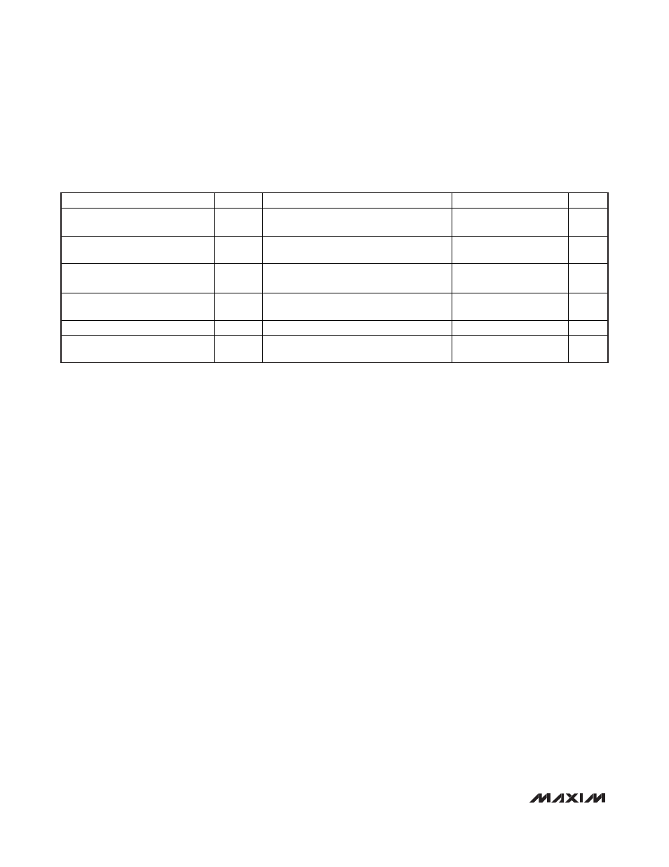
MISCELLANEOUS TIMING CHARACTERISTICS (Note 15) (continued)
(DV
DD
= +2.7V to +5.25V, AV
DD
= +4.75V to +5.25V, V
DGND
= V
AGND
= 0, external V
REFADC
= +2.5V, external V
REFDAC
= +2.5V,
C
REF
= 0.1µF, T
A
= -40°C to +85°C, unless otherwise noted.)
PARAMETER
SYMBOL
CONDITIONS
MIN
TYP
MAX
UNITS
DAC Power-Up Time (External
Reference)
t
DPUEXT
2
µs
DAC Power-Up Time (Internal
Reference)
t
DPUINT
70
µs
Acquisition Time (Internally Timed
in ADC Clock Modes 00 or 01)
t
ACQ
0.6
µs
Conversion Time (Internally
Clocked)
t
CONV
Internally clocked, T
A
= +25°C
10
µs
Delay to Start of Conversion Time
t
CONVW
(Note 23)
1.3
µs
Temperature Conversion Time
(Internally Clocked)
t
CONVT
70
µs
Note 1: Output settles to within ±0.5% of final value.
Note 2: Total unadjusted errors are for the entire gate-drive channel including the 12-bit DAC, and the gate driver is measured at
the GATE1 and GATE2 outputs.
Note 3: V
GATE_
= V
DD
- 0.1. Measured from when OPSAFE1 or OPSAFE2 is set high.
Note 4: During power-on-reset, the output safe switch is closed. The output safe switch is opened under user software control.
Note 5: Guaranteed to be 11 bits linearly accurate.
Note 6: Offset nulled.
Note 7: The absolute range for analog inputs is from 0 to V
AVDD
.
Note 8: Internal temperature-sensor performance is guaranteed by design.
Note 9: The MAX11008 and the external sensor are at the same ambient temperature. External sensor measurement error is tested
with a diode-connected 2N3904.
Note 10: Guaranteed monotonicity. Accuracy is degraded at lower V
REFDAC
.
Note 11: SDA/DIN is an open-drain output only when in I
2
C mode. A1/DOUT is an open-drain output only when in SPI mode.
Note 12: Supply-current limits are valid only when digital inputs are set to DGND or supply voltage. Timing specifications are only
guaranteed when inputs are driven rail-to-rail.
Note 13: Shutdown supply currents are typically 0.4µA for AV
DD
; maximum specification is limited by automated test equipment.
Note 14: All times are referred to the 50% point between V
IH
and V
IL
levels.
Note 15: Guaranteed by design. Not production tested.
Note 16: DOUT will go into three-state mode after the
CS rising edge. Keep CS low long enough for the DOUT value to be sampled
before it goes to three-state.
Note 17: A master device must provide a hold time of at least 300ns for the SDA signal (referred to V
IL
of the SCL signal) to bridge
the undefined region of SCL’s falling edge.
Note 18: t
R
and t
F
measured between 0.3 x DV
DD
and 0.7 x DV
DD
.
Note 19: C
B
= total capacitance of one bus line in pF. For bus loads between 100pF and 400pF, the timing parameters should be
linearly interpolated.
Note 20: An appropriate bus pullup resistance must be selected depending on board capacitance.
Note 21: Input filters on the SDA and SCL inputs suppress noise spikes less than 50ns.
Note 22: When a command is written to the serial interface, the command is passed by the internal oscillator clock and executed.
There is a small synchronization delay before the new value is written to the appropriate register. If the serial interface
attempts to read the new value back before t
RDBK
, the new data is not corrupted; however, the result of the read command
may not reflect the new value.
Note 23: This is the minimum time from the end of a command before
CNVST should be asserted. The time allows for the data from
the preceding write to arrive and set up the chip in preparation for the
CNVST. The time need only be observed when the
write affects the ADC controls. Failure to observe this time may lead to incorrect conversions (for example, conversion of
the wrong ADC channel).
