Rainbow Electronics MAX11008 User Manual
Page 22

MAX11008
MAX11008 returns to F/S mode. Use a repeated START
condition in place of a STOP condition to leave the bus
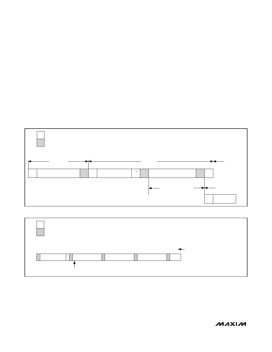
active and the mode unchanged. Figure 9 summarizes
the data bit transfer format for HS-mode communication.
Register Address/Data Bytes (Write Cycle)
A write cycle begins with the bus master issuing a
START condition followed by 7 address bits (see Figure
5 and Table 1) and a write bit (R/
W = 0). Once the
slave address is recognized and the write bit is
received, the MAX11008 (I
2
C slave) issues an ACK by
pulling SDA low for one clock cycle. The master then
sends the register address byte (command byte) to the
slave. The MSB of the register address byte is the
read/write bit for the destination register address of the
slave and must be set to 0 for a write cycle (see the
Register Address Map
section). After receiving the
byte, the slave issues another acknowledge, pulling
SDA low for one clock cycle. The master then writes
two data bytes, receiving an ACK from the slave after
each byte is sent. The master ends the write cycle by
issuing a STOP condition. When operating in HS mode,
a STOP condition returns the bus into F/S mode (see
the
HS I
2
C Mode
section). Figure 10 shows a complete
write cycle.
Dual RF LDMOS Bias Controller with
Nonvolatile Memory
22
______________________________________________________________________________________
S
MASTER CODE
N
Sr
SLAVE ADDRESS
R/W
A
DATA
A
P
Sr
SLAVE ADD
F/S MODE
HS MODE
N BYTES + ACK
HS MODE CONTINUES
F/S MODE
MASTER TO SLAVE
SLAVE TO MASTER
Figure 9. Data-Transfer Format in HS Mode
SLAVE TO MASTER
MASTER TO SLAVE
S
1
SLAVE
ADDRESS
A
7
1 1
W
REGISTER ADDRESS
BYTE
8
P OR Sr
1
MSB DETERMINES
WHETHER TO READ OR WRITE TO
REGISTERS
4-BYTE WRITE CYCLE
NUMBER OF BITS
A
1
DATA BYTE
8
A
1
DATA BYTE
8
A
1
Figure 10. Write Cycle
