Table 11d. clock mode and cnvst bit (cksel[1:0]) – Rainbow Electronics MAX11008 User Manual
Page 49
MAX11008
Dual RF LDMOS Bias Controller with
Nonvolatile Memory
______________________________________________________________________________________
49
PG_SET1
PG_SET0
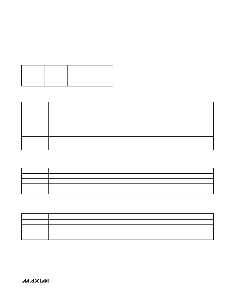
PGA GAIN
0
0
2
0
1
10
1
X
25
Table 11c. PGA1 and PGA2 Gain Setting
Bits (PG_SET[1:0])
CKSEL1
CKSEL0
ADC CONVERSION TYPE
0
0
Internally timed acquisitions and conversions start by writing to the ADC Conversion register
and enabling one or more channels. See the ADC Conversion Register (ADCCON) (Write
Only) section. All of the selected channels are sequentially converted each time the ADC
Conversion register is written to.
0
1
Internally timed acquisitions and conversions start by asserting a low pulse at
CNVST
whenever one or more channels are enabled in the ADC Conversion register. All of the
selected channels are sequentially converted each time a low pulse is asserted at
CNVST.
1
0
Reserved. Do not use.
1
1
Selected channels are converted individually each time
CNVST is pulled low. Each low pulse
on
CNVST converts the next channel in the sequence.
Table 11d. Clock Mode and
CNVST Bit (CKSEL[1:0])
ADCREF1
ADCREF0
ADC REFERENCE
0
X
ADC uses external reference voltage supplied at the ADCREF input.
1
0
ADC uses internal reference voltage.
1
1
ADC uses internal reference voltage. Connect external decoupling capacitor at REFADC for
better noise performance.
Table 11e. ADC Reference Configuration Bits (ADCREF[1:0])
X = Don’t care.
X = Don’t care.
DACREF1
DACREF0
DAC REFERENCE
0
X
DAC uses external reference voltage supplied at the DACREF input.
1
0
DAC uses internal reference voltage.
1
1
DAC uses internal reference voltage. Connect external decoupling capacitor at REFDAC for
better noise performance.
Table 11f. DAC Reference Configuration Bits (DACREF[1:0])
X = Don’t care.
X = Don’t care.