Chip information, Package information, Pin configuration – Rainbow Electronics MAX11008 User Manual
Page 67: Spurious-free dynamic range, Intermodulation distortion (imd), Full-power bandwidth
MAX11008
Dual RF LDMOS Bias Controller with
Nonvolatile Memory
Maxim cannot assume responsibility for use of any circuitry other than circuitry entirely embodied in a Maxim product. No circuit patent licenses are
implied. Maxim reserves the right to change the circuitry and specifications without notice at any time.
Maxim Integrated Products, 120 San Gabriel Drive, Sunnyvale, CA 94086 408-737-7600 ____________________ 67
© 2008 Maxim Integrated Products
Maxim is a registered trademark of Maxim Integrated Products, Inc.
Spurious-Free Dynamic Range
Spurious-free dynamic range (SFDR) is the ratio of the
RMS amplitude of the fundamental (maximum signal
component) to the RMS value of the next largest spec-
tral component.
Intermodulation Distortion (IMD)
IMD is the total power of the intermodulation products
relative to the total input power when two tones, f1 and
f2, are present at the inputs. The intermodulation prod-
ucts are (f1 ± f2), (2 x f1), (2 x f2), (2 x f1 ± f2), (2 x f2 ±
f1). The individual input tone levels are at -7dB FS.
Full-Power Bandwidth
A large -0.5dB FS analog input signal is applied to an
ADC, and the input frequency is swept up to the point
where the amplitude of the digitized conversion result
has decreased by -3dB. This point is defined as the
full-power input bandwidth frequency.
Chip Information
PROCESS: BiCMOS
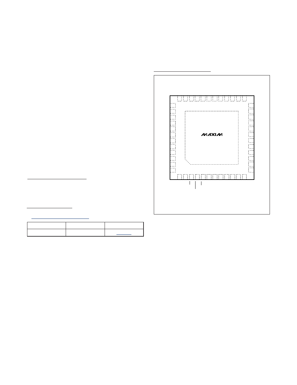
Package Information
For the latest package outline information and land patterns, go
to
www.maxim-ic.com/packages
.
PACKAGE TYPE
PACKAGE CODE
DOCUMENT NO.
48 TQFN-EP
T4877M-1
TOP VIEW
MAX11008
THIN QFN
7mm x 7mm x 0.8mm
13
14
15
16
17
18
19
20
21
22
23
24
DXN2
ADCIN1
ADCIN2
PGAOUT2
GATE2
GATE1
N.C.
AV
DD
AGND
AGND
AGND
AV
DD
48
47
46
45
44
43
42
41
40
39
38
37
1
2
3
4
5
6
7
8
9
10
11
12
N.C.
DV
DD
BUSY
A1/DOUT
SDA/DIN
SCL/SCLK
N.C.
A2/N.C.
PGAOUT1
N.C.
N.C.
N.C.
DXP2
DXN1
DXP1
REFADC
REFDAC
OPSAFE2
ALARM
SPI/I2C
CNVST
A0/CS
OPSAFE1
DGND
36
35
34
33
32
31
30
29
28
27
26
25
N.C.
CS2+
CS2-
CS1-
CS1+
N.C.
DGND
DV
DD
DV
DD
N.C.
N.C.
N.C.
EP*
*EP = EXPOSED PAD.
+
Pin Configuration