Rainbow Electronics MAX11008 User Manual
Page 24

MAX11008
12-Bit ADC
The MAX11008 12-bit ADC uses a SAR conversion
technique and on-chip track-and-hold (T/H) circuitry to
convert the PGA outputs (PGAOUT1 and PGAOUT2),
temperature measurements, and single-ended auxiliary
input voltages (ADCIN1 and ADCIN2) into 12-bit digital
data when in ADC monitor mode (see the
Hardware
Configuration Register (HCFIG) (Read/Write)
section).
All nontemperature measurements are converted using
a unipolar transfer function (see Figure 13), and all tem-
perature measurements are converted using a bipolar
transfer function (see Figure 14).
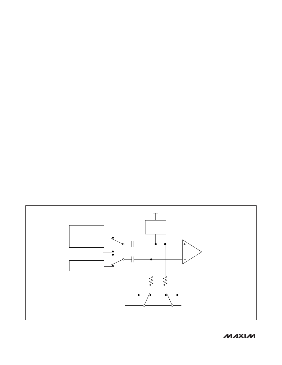
Analog Input T/H
Figure 12 shows the equivalent circuit for the ADC input
architecture of the MAX11008. In track mode, an input
capacitor is connected to the input signal (ADCIN1,
ADCIN2, PGAOUT1, PGAOUT2, or temperature sensor
processor output). Another input capacitor is connect-
ed to AGND. After the T/H enters hold mode, the differ-
ence between the sampled positive and negative input
voltages is converted. The charging rate of the input
capacitance determines the time required for the T/H to
acquire an input signal. If the input signal’s source
impedance is high, the required acquisition time
lengthens accordingly.
Any source impedance below 300Ω does not affect the
ADC’s AC performance. A high-impedance source can
be accommodated either by lengthening t
ACQ
or by
placing a 1µF capacitor between the positive and neg-
ative analog inputs. The combination of the analog-
input source impedance and the capacitance at the
analog input creates an RC filter that limits the analog
input bandwidth.
Input Bandwidth
The ADC’s input-tracking circuitry has a 1MHz small-
signal bandwidth, to digitize high-speed transient
events and measure periodic signals with bandwidths
exceeding the ADC’s sampling rate by using under-
sampling techniques. Anti-alias filtering of the input sig-
nals is necessary to prevent high-frequency
components from aliasing into the frequency band of
interest.
Analog Input Protection
Internal electrostatic-discharge (ESD) protection diodes
clamp all analog inputs to AV
DD
and AGND, allowing
the inputs to swing from (AGND - 0.3V) to (AV
DD
+
0.3V) without damage. However, for accurate conver-
sions near full scale, the inputs must not exceed AV
DD
by more than 50mV or be lower than AGND by 50mV. If
an analog input voltage exceeds the supplies, limit the
input current to 2mA.
Dual RF LDMOS Bias Controller with
Nonvolatile Memory
24
______________________________________________________________________________________
HOLD
HOLD
HOLD
CAPACITIVE
DAC
REFADC
CIN+
CIN-
TRACK
AGND
ADCIN1
ADCIN2
PGAOUT1
PGAOUT2
TEMP SENSOR READING
TRACK
TRACK
ALL SWITCHES SHOWN IN TRACK MODE.
COMPARATOR
AV
DD
/2
Figure 12. Analog Input Track and Hold
