Detailed description, Digital serial interface – Rainbow Electronics MAX11008 User Manual
Page 17

Detailed Description
The MAX11008 sets and controls the bias conditions
for dual RF LDMOS power devices found in cellular
base-station power amps. Each device includes two
high-side current-sense amplifiers with programmable
gains of 2, 10, and 25 to monitor the LDMOS transistor
drain current over the 20mA to 5A range. Two external
diode-connected transistors monitor the LDMOS tran-
sistor temperatures while an internal temperature sen-
sor measures the local die temperature of the
MAX11008. The 12-bit ADC is interfaced to a 7:1 multi-
plexer and converts the signals from the PGA outputs,
internal and external temperature readings, or the two
auxiliary analog inputs into digital data results that can
be stored in the FIFO.
On the control side, two gate-drive channels, driven
from two 12-bit DACs and a gain stage of 2, generate a
positive gate voltage bias for the LDMOS. Each gate-
drive output supports up to ±2mA of gate current. The
gate-drive amplifier is current-limited to ±25mA and
features a fast clamp to analog ground that operates
independently of the serial interface.
The MAX11008 includes an on-chip, nonvolatile
EEPROM that stores LUTs and register information. The
LUTs are designed to store gate voltage vs. temperature
curves for the LDMOS FET. The data is used for temper-
ature compensation of the LDMOS FET’s bias point.
The LUTs can also contain compensation data for anoth-
er independent parameter: either sense voltage or
AIN voltage.
Digital Serial Interface
The MAX11008 features both an I
2
C and an SPI-com-
patible serial interface. Connect SPI/
I2C to DGND to
select the I
2
C serial-interface operation, or to DV
DD
to
select the SPI serial-interface operation. Do not alter
interface mode during operation.
SPI Serial Interface
Connect SPI/
I2C to DV
DD
to select the SPI interface.
The SPI serial interface consists of a serial data input
(DIN), a serial clock line (SCLK), a chip select (
CS),
and a serial data output (DOUT). The use of serial data
output (DOUT) is optional and is only required when
data is to be read back by the master device. The
MAX11008 is SPI compatible within the range of V
DD
=
+2.7V to +5.25V. DIN, SCLK,
CS, and DOUT facilitate
bidirectional communication between the MAX11008
and the master at rates up to 20MHz.
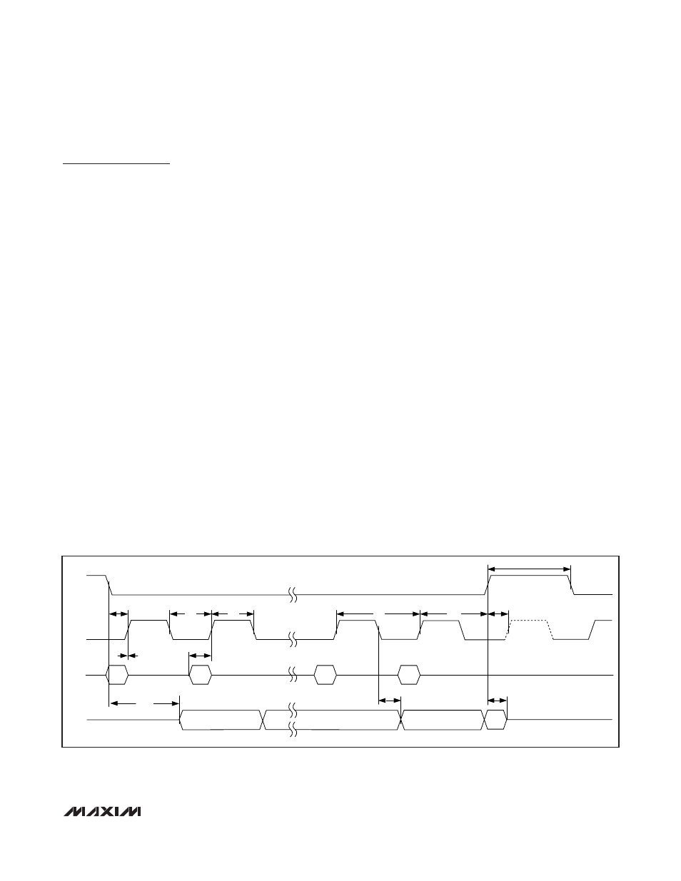
Figure 1 illustrates the 4-wire interface timing diagram.
The MAX11008 is a transmit/receive slave-only device,
relying upon a master to generate a clock signal. The
master initiates data transfer on the bus and generates
the SCLK signal to permit data transfer.
MAX11008
Dual RF LDMOS Bias Controller with
Nonvolatile Memory
______________________________________________________________________________________
17
t
CSS
SCLK
t
DH
t
DV
t
DS
CS
DIN
DOUT
D23
D22
D1
D0
t
CH
t
CSH
t
CSS
t
CSW
t
CL
t
CP
t
DO
t
TR
Figure 1. SPI Serial-Interface Timing
