Table 2. order of adc conversion scan, Internally timed acquisitions and conversions – Rainbow Electronics MAX11008 User Manual
Page 25

ADC Transfer Functions
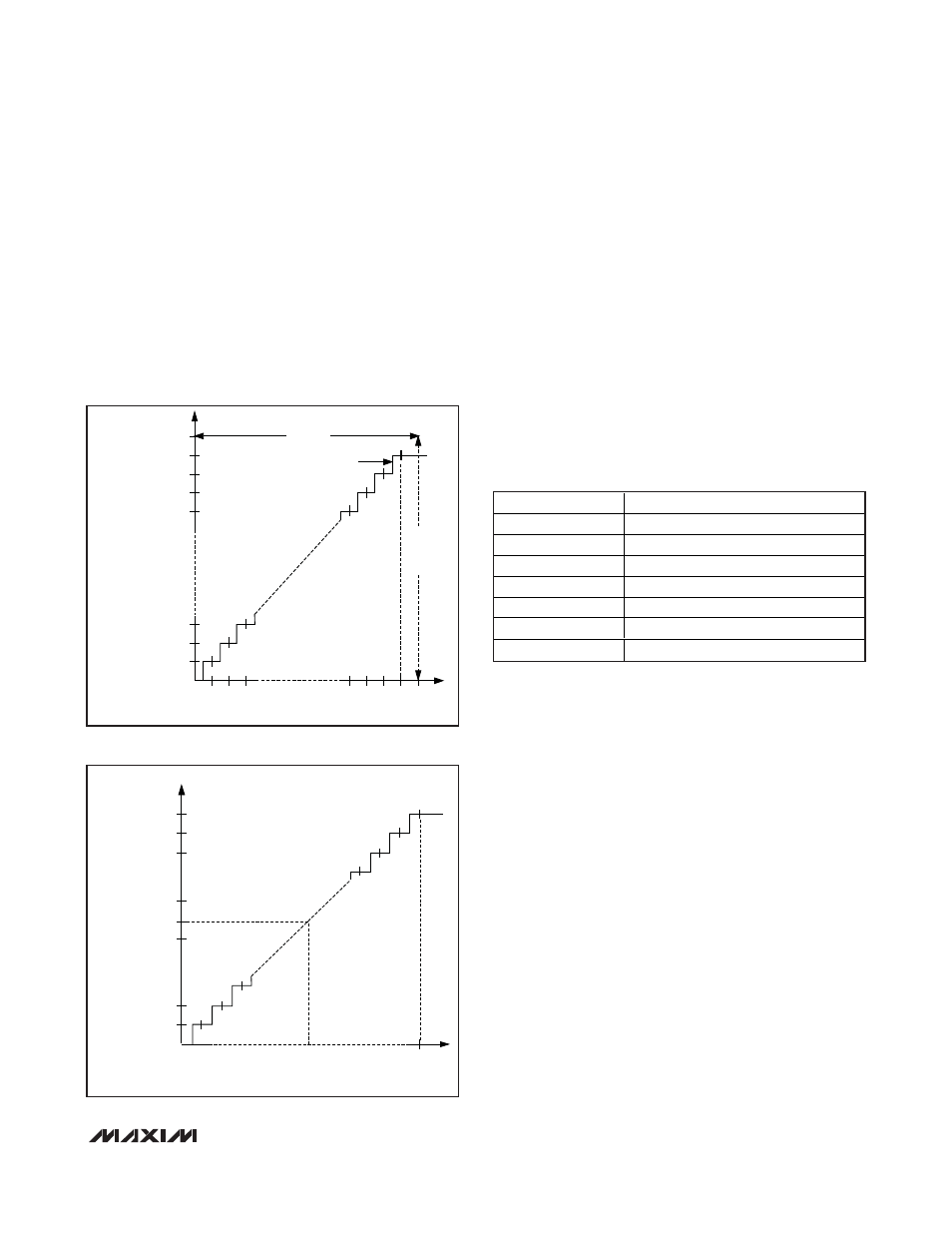
Figure 13 shows the unipolar transfer function for non-
temperature measurements, and Figure 14 shows the
bipolar transfer function used for temperature measure-
ments. Code transitions occur halfway between suc-
cessive-integer LSB values. Output coding is binary,
with 1 LSB = V
REFADC
/4096 for nontemperature mea-
surements, and 1 LSB = +0.125°C for temperature
measurements. All signed binary results use two’s com-
plement format.
ADC Conversion Scheduling
The MAX11008 ADC multiplexer scans and converts
the selected inputs in the order shown in Table 2 (see
the
ADC Conversion Register (ADCCON) (Write Only)
section) when more than one channel is selected. The
results are stored in the FIFO when in ADC monitoring
mode. The BUSY signal is set at the start and reset at
the end of a scan except when the continuous convert
bit is set at which time BUSY does not then respond to
ADC conversions.
Writing a conversion command before a conversion is
complete cancels the pending conversion. Avoid
addressing the device using the serial interface while
the ADC is converting.
ADC Clock Modes
The MAX11008 offers three conversion/acquisition
modes (known as clock modes) selectable through
configuration register bits CKSEL1 and CKSEL0.
If the ADC conversion requires the internal reference
(temperature measurement or voltage measurement with
internal reference selected) and the reference has not
been previously forced on (FBGON = 1), the device
inserts a typical delay of 72µs, for the reference to settle,
before commencing the ADC conversion. The reference
remains powered up while there are pending conver-
sions. If the reference is not forced on, it automatically
powers down at the end of a scan or when CONCONV in
the ADC Conversion register is set back to 0.
Internally Timed Acquisitions
and Conversions
Clock Mode 00
In clock mode 00, power-up, acquisition, conversion,
and power-down are all initiated by writing to the ADC
Conversion register and performed automatically using
the internal oscillator. This is the default clock mode.
The ADC sets the BUSY output high, powers up, and
scans all requested channels storing the results in the
FIFO if the ADCMON bit has been set. After the scan is
MAX11008
Dual RF LDMOS Bias Controller with
Nonvolatile Memory
______________________________________________________________________________________
25
FULL-SCALE TRANSITION
INPUT VOLTAGE (LSB)
BINAR
Y OUTPUT CODE
0
0000 0000 0001
0000 0000 0000
0000 0000 0010
0000 0000 0011
1111 1111 1101
1111 1111 1100
1111 1111 1110
1111 1111 1111
1 LSB = V
REFADC
/4096
1
2
3
4093
4095
V
REFADC
V
REF
ADC
Figure 13. ADC Transfer Function
TEMPERATURE (°C)
OUTPUT CODE
-256
+255
0
1000 0000 0000
1000 0000 0001
0000 0000 0001
0111 1111 1111
0111 1111 1110
0111 1111 1101
0000 0000 0000
1111 1111 1111
1000 0000 0010
1 LSB = +0.125°C
Figure 14. Temperature Transfer Function
ORDER OF SCAN
DESCRIPTION OF CONVERSION
1
Internal device temperature
2
External diode 1 temperature
3
Output of PGA 1 for current sense
4
Auxiliary input 1 (ADCIN1)
5
External diode 2 temperature
6
Output of PGA 2 for current sense
7
Auxiliary input 2 (ADCIN2)
Table 2. Order of ADC Conversion Scan
