Read format, C serial interface, Bus timing – Rainbow Electronics MAX11008 User Manual
Page 19: Hs i, C mode, Connect spi/ i2c to dgnd to select the i, C interface. the i, C com- patible within the dv

Read Format
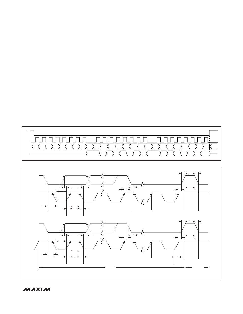
Use the following sequence to read 16 bits of data from
a MAX11008 register (see Figure 3):
1) Drive
CS low to select the device.
2) Send the appropriate read command byte (see
Table 6 for the register address map). The com-
mand byte is clocked in on the rising edges of
SCLK.
3) Receive 16 bits of data. The first 4 bits of data are
always high. Data is clocked out on the falling edges
of SCLK.
4) Drive
CS high.
I
2
C Serial Interface
Connect SPI/
I2C to DGND to select the I
2
C interface. The
I
2
C serial interface consists of a serial data line (SDA)
and a serial clock line (SCL). The MAX11008 is I
2
C com-
patible within the DV
DD
= 2.7V to 5.25V range. SDA and
SCL facilitate bidirectional communication between the
MAX11008 and the master at rates up to 400kHz for fast
mode and up to 3.4MHz for high-speed mode (HS
mode). See the
Bus Timing
and
HS I
2
C Mode
sections
for more information on data-rate configurations.
Figure 4 shows the 2-wire interface timing diagram. The
MAX11008 is a transmit/receive slave-only device, rely-
ing upon a master to generate a clock signal. The mas-
ter (typically a microcontroller) initiates data transfers
on the bus and generates the SCL signal to permit data
transfer.
MAX11008
Dual RF LDMOS Bias Controller with
Nonvolatile Memory
______________________________________________________________________________________
19
SCLK
C6
R/W
C4
C5
C2
C3
C0
C1
DIN
CS
DOUT
D14
D13
D12
D11
D10
D9
D8
D6
D5
D4
D3
D2
D1
D15
D7
D0
X
X
X
X
X
X
X
X
X
X
X
X
X
X
X
X
X
X
Figure 3. SPI Read Sequence
SDA
SCL
t
SU, DAT
t
HD, STA
t
HD, STA
t
RCL
t
LOW
t
HIGH
t
R
t
F
t
HIGH
t
RCL
t
LOW
t
SU, DAT
t
HD, DAT
t
HD, DAT
t
HD, STA
t
R
t
F
t
BUF
t
BUF
t
RDA
t
RDA
t
RCL
t
HD, STA
t
SU, STA
t
SU, ST0
t
SU, ST0
t
SU, STA
SCL
S
Sr
A
Sr
A
P
S
P
F/S MODE
HS MODE
S
S
SDA
a) F/S-MODE I
2
C SERIAL INTERFACE TIMING
b) HS-MODE I
2
C SERIAL INTERFACE TIMING
PARAMETERS ARE MEASURED FROM 30% TO 70%.
Figure 4. I
2
C Serial-Interface Timing Diagram
