Rainbow Electronics MAX11008 User Manual
Page 18
MAX11008
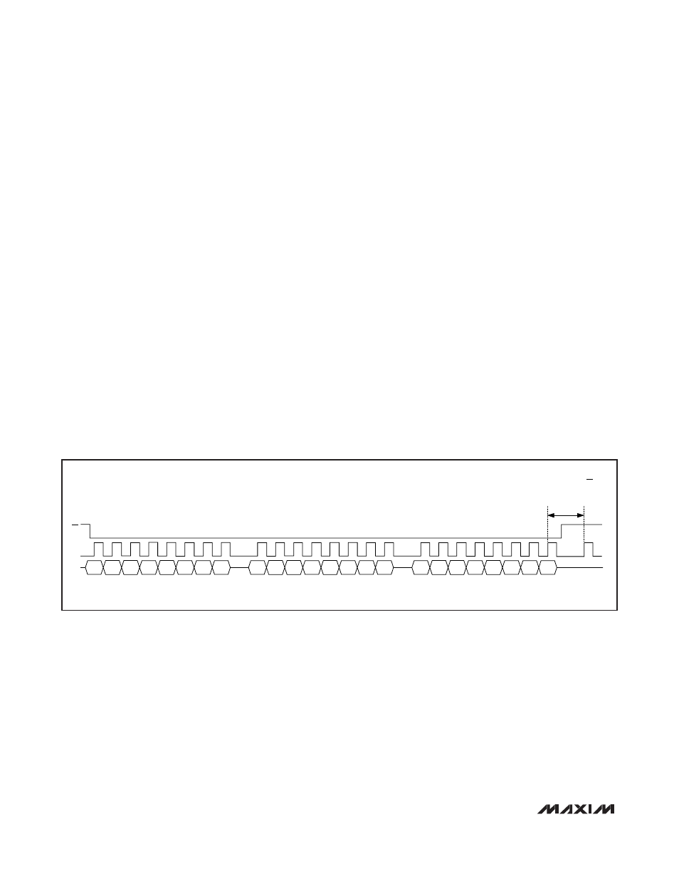
The SPI bus cycles are 24 bits long. Data can be sup-
plied as three 8-bit bytes or as a continuous 24-bit
stream.
CS must remain low throughout the 24-bit
sequence. The first 8-bit byte is a command byte
C[7:0]. The next 16 bits are data bits D[15:0]. Clock
signal SCLK can idle low or high, but data is always
clocked in on the rising edge of SCLK (CPOL = CPHA).
SPI data transfers begin with the falling edge of
CS.
Data is clocked into the device on the rising edges of
SCLK and clocked out of the device on the falling
edges of SCLK. For correct bus cycles,
CS should
frame the data and should not return to a 1 until after
the last active rising clock edge. See Figure 2 for timing
details. A rising edge of
CS causes DOUT to three-
state and data reads should be performed accordingly.
See Figures 1 and 3.
When writing instructions to the MAX11008, 24 clock
cycles must be completed before
CS is driven high.
The MAX11008 executes the instruction only after the
24th clock cycle has been received and
CS is driven
high. To abort unwanted instructions,
CS can be driven
high at any time before the 23rd rising clock edge.
When reading data from the MAX11008, 24 clock
cycles must be completed before
CS is driven high. If
CS is driven high before the completion of the 24th
falling edge, DOUT immediately three-states, the inter-
face resets in preparation for the next command, and
the data being read is lost.
Write Format
Use the following sequence to write 16 bits of data to a
MAX11008 register (see Figure 2):
1) Drive
CS low to select the device.
2) Send the appropriate write command byte (see
Table 6 for the register address map). The com-
mand byte is clocked in on the rising edge of SCLK.
3) Send 16 bits of data D[15:0] starting with the most
significant bit (MSB). Data is clocked in on the rising
edges of SCLK.
4) Drive
CS high to conclude the command.
Dual RF LDMOS Bias Controller with
Nonvolatile Memory
18
______________________________________________________________________________________
SCLK
C6
CR/W-
C4
C5
C2
C3
C0
C1
DIN
D15
D14
D13
D12
D11
D10
D9
D8
D7
D6
D5
D4
D3
D2
D1
D0
CS
A RISING EDGE OF CS
DURING THIS PERIOD
COMPLETES A VALID WRITE
COMMAND
Figure 2. SPI Write Sequence