Rf01 – Rainbow Electronics RF01 User Manual
Page 19
RF01
minimize these errors it is suggested to use the same crystal type and the same PCB layout for the
crystal placement on the RX and TX PCBs.
To verify the possible RX-TX offset it is suggested to measure the CLK output of both chips with a
high level of accuracy. Do not measure the output at the XTL pin since the measurement process itself
will change the reference frequency. Since the carrier frequencies are derived from the reference
frequency, having identical reference frequencies and nominal frequency settings at the TX and RX side
there should be no offset if the CLK signals have identical frequencies.
It is possible to monitor the actual RX-TX offset using the AFC status report included in the status
byte of the receiver. By reading out the status byte from the receiver the actual measured offset
frequency will be reported. In order to get accurate values the AFC has to be disabled during the read by
clearing the "en" bit in the AFC Control Command (bit 0).
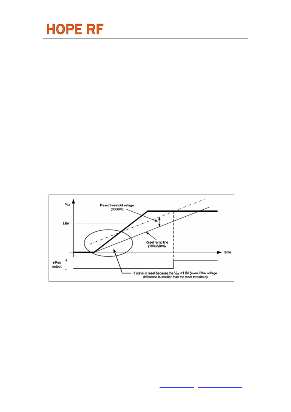
Power-on reset
After power up the supply voltage starts to rise from 0V. The reset block has an internal ramping voltage
reference (reset-ramp signal), which is rising at 100mV/ms (typical) rate. The chip remains in reset state while
the voltage difference between the actual V
dd
and the internal reset-ramp signal is higher than the reset
threshold voltage, which is 600 mV (typical). As long as the V
dd
voltage is less than 1.6V (typical)
the chip stays in reset mode regardless the voltage difference between the V
dd
and the internal ramp signal.
The reset event can last up to 150ms supposing that the V
dd
reaches 90% its final value within 1ms. During this
period the chip does not accept control commands via the serial control interface.
Power-on reset example:
Power glitch reset
The internal reset block has two basic mode of operation: normal and sensitive reset. The default mode is
sensitive, which can be changed by the appropriate control command (see Related control commands at the
end of this section). In normal mode the power glitch detection circuit is disabled.
There can be spikes or glitches on the V
dd
line if the supply filtering is not satisfactory or the internal resistance
of the power supply is too high. In such cases if the sensitive reset is enabled an (unwanted) reset will be
generated if the positive going edge of the V
dd
has a rising rate greater than 100mV/ms and the voltage
difference between the internal ramp signal and the V
dd
reaches the reset threshold voltage (600 mV). Typical
case when the battery is weak and due to its increased internal resistance a sudden decrease of the current
consumption (for example turning off the power amplifier) might lead to an increase in supply voltage. If for
some reason the sensitive reset cannot be disabled step-by-step decrease of the current consumption (by
turning off the different stages one by one) can help to avoid this problem.
Tel: +86-755-86096587 Fax: +86-755-86096602 E-mail: [email protected] http://www.hoperf.com