Rf01, Rx-tx alignment procedures – Rainbow Electronics RF01 User Manual
Page 18
RF01
CRL
Clock recovery lock
ATGL
Toggling in each AFC cycle
ASAME
AFC stablized (measured twice the same offset value)
OFFS6, 4-0 Offset value to be add to the value of the Frequency control word
FIFO Buffered Data Read
In this operating mode, incoming data are clocked into a 16 bit FIFO buffer. The receiver starts to fill
up the FIFO when the Valid Data Indicator (VDI) bit and/or the synchron word recognition circuit indicates
potentially real incoming data. This prevents the FIFO from being filled with noise and overloading the
external microcontroller.
For further details see the Receiver Setting Command and the Output and FIFO Command.
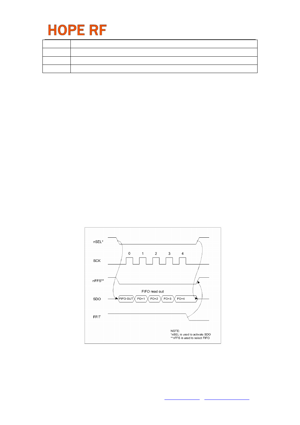
Polling Mode:
The nFFS signal selects the buffer directly and its content could be clocked out through pin SDO by
SCK. Set the FIFO IT level to 1. In this case, as long as FFIT indicates received bits in the FIFO, the
controller may continue to take the bits away. When FFIT goes low, no more bits need to be taken. An
SPI read command is also available.
Interrupt Controlled Mode:
The user can define the FIFO level (the number of received bits) which will generate the nFFIT when
exceeded. The status bits report the changed FIFO status in this case.
FIFO Read Example with FFIT Polling:
During FIFO access the f
SCK
cannot be higher than f
ref
/4, where f
ref
is the crystal oscillator frequency.
RX-TX ALIGNMENT PROCEDURES
RX-TX frequency offset can be caused only by the differences in the actual reference frequency. To
Tel: +86-755-86096587 Fax: +86-755-86096602 E-mail: [email protected] http://www.hoperf.com