Chip information, Package information, Table 52. circular buffer readout sequence – Rainbow Electronics MAX5961 User Manual
Page 42
MAX5961
0 to 16V, Quad, Hot-Swap Controller
with 10-Bit Current and Voltage Monitor
Maxim cannot assume responsibility for use of any circuitry other than circuitry entirely embodied in a Maxim product. No circuit patent licenses are
implied. Maxim reserves the right to change the circuitry and specifications without notice at any time.
42 ____________________Maxim Integrated Products, 120 San Gabriel Drive, Sunnyvale, CA 94086 408-737-7600
© 2008 Maxim Integrated Products
is a registered trademark of Maxim Integrated Products, Inc.
Receive Byte
The receive byte protocol allows the master device to
read the register content of the MAX5961 (see Figure
8). The EEPROM or register address must be preset
with a send byte protocol first. Once the read is com-
plete, the internal pointer increases by one. Repeating
the receive byte protocol reads the contents of the next
address. The receive byte procedure follows:
1) The master sends a START condition.
2) The master sends the 7-bit slave address and a
read bit (high).
3) The addressed slave asserts an ACK on SDA.
4) The slave sends 8 data bits.
5) The slave increments its internal address pointer.
6) The master asserts an ACK on SDA and repeats
steps 4 and 5 or asserts a NACK and generates a
STOP condition.
The internal address pointer returns to 0x00 after incre-
menting from the highest register address.
Address Pointers
Use the send byte protocol to set the register address
pointers before read and write operations. For the con-
figuration registers, valid address pointers range from
0x00 to 0x74, and the circular buffer addresses are
0x80 to 0x87. Register addresses outside this range
result in a NACK being issued from the MAX5961.
Circular Buffer Read
The circular buffer read operation is similar to the
receive byte operation. The read operation is triggered
after any one of the circular buffer base addresses is
loaded. During a circular buffer read, although all is
transparent from the external world, internally the
autoincrement function in the I
2
C controller is disabled.
Thus, it is possible to read one of the circular buffer
blocks with a burst read without changing the virtual
internal address corresponding to the base address.
Once the master issues a NACK, the circular reading
stops, and the default functions of the I
2
C slave bus
controller are restored.
In 8-bit read mode, every I
2
C read operation shifts out
a single sample from the circular buffer. In 10-bit mode,
two subsequent I
2
C read operations shift out a single
10-bit sample from the circular buffer, with the high-
order byte read first, followed by a byte containing the
right-shifted 2 LSBs. Once the master issues a NACK,
the read circular buffer operation terminates and nor-
mal I
2
C operation returns.
The data in the circular buffers is read back with the
next-to-oldest sample first, followed by progressively
more recent samples until the most recent sample is
retrieved, followed finally by the oldest sample (see
Table 52).
Chip Information
PROCESS: BiCMOS
Table 52. Circular Buffer Readout Sequence
READ-OUT ORDER
1st
OUT
2nd OUT
…
48th OUT
49th OUT
50th OUT
Chronological Number
1
2
…
48
49
0
Package Information
For the latest package outline information, go to
www.maxim-ic.com/packages
.
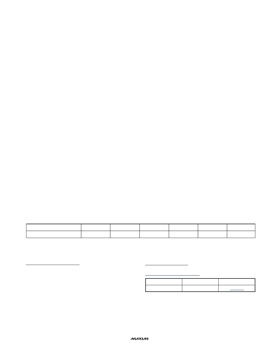
PACKAGE TYPE
PACKAGE CODE
DOCUMENT NO.
48 TQFN
T4877-6