Table 51. slave address settings – Rainbow Electronics MAX5961 User Manual
Page 38
MAX5961
0 to 16V, Quad, Hot-Swap Controller
with 10-Bit Current and Voltage Monitor
38
______________________________________________________________________________________
I
2
C Serial Interface
The MAX5961 features an I
2
C-compatible serial interface
consisting of a serial-data line (SDA) and a serial-clock
line (SCL). SDA and SCL allow bidirectional communica-
tion between the MAX5961 and the master device at
clock rates from 100kHz to 400kHz. The I
2
C bus can
have several devices (e.g., more than one MAX5961, or
other I
2
C devices in addition to the MAX5961) attached
simultaneously. The A0 and A1 inputs set one of nine
possible I
2
C addresses (see Table 51).
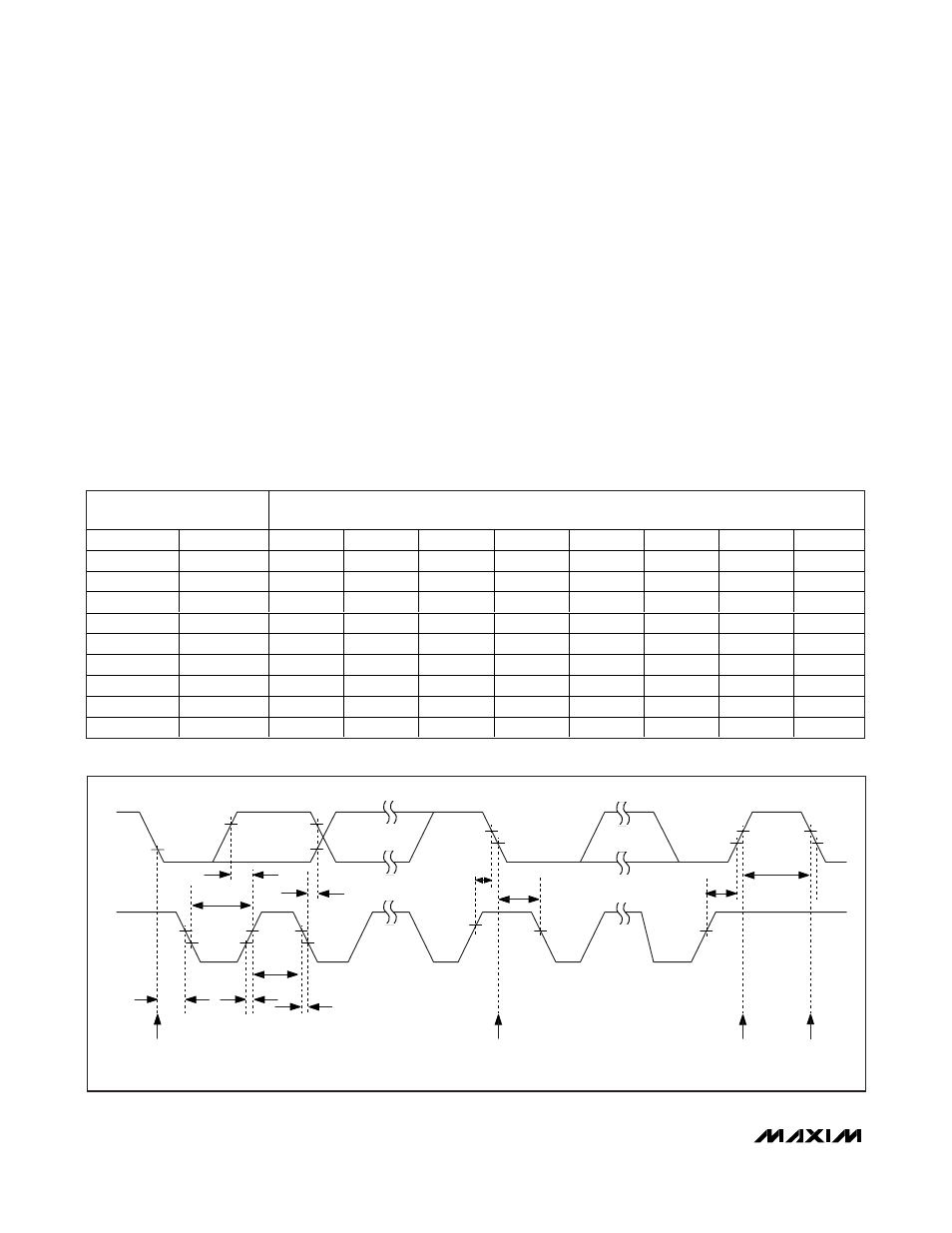
The 2-wire communication is fully compatible with exist-
ing 2-wire serial-interface systems; Figure 5 shows the
interface timing diagram. The MAX5961 is a
transmit/receive slave-only device, relying upon a mas-
ter device to generate a clock signal. The master
device (typically a µC) initiates data transfer on the bus
and generates SCL to permit that transfer.
A master device communicates to the MAX5961 by
transmitting the proper address followed by command
and/or data words. Each transmit sequence is framed
by a START (S) or REPEATED START (SR) condition
and a STOP (P) condition. Each word transmitted over
the bus is 8 bits long and is always followed by an
acknowledge pulse.
SCL is a logic input, while SDA is a logic-input/open-
drain output. SCL and SDA both require external pullup
resistors to generate the logic-high voltage. Use 4.7kΩ
for most applications.
Table 51. Slave Address Settings
ADDRESS INPUT STATE
I
2
C ADDRESS BITS
A1
A0
ADDR 7
ADDR 6
ADDR 5
ADDR 4
ADDR 3
ADDR 2
ADDR 1
ADDR 0
Low
Low
0
1
1
1
0
1
0
R/W
Low
High
0
1
1
1
0
0
1
R/W
Low
Unconnected
0
1
1
1
0
0
0
R/W
High
Low
0
1
1
0
1
1
0
R/W
High
High
0
1
1
0
1
0
1
R/W
High
Unconnected
0
1
1
0
1
0
0
R/W
Unconnected
Low
0
1
1
0
0
1
0
R/W
Unconnected
High
0
1
1
0
0
0
1
R/W
Unconnected Unconnected
0
1
1
0
0
0
0
R/W
Figure 5. Serial-Interface Timing Details
STOP
CONDITION
REPEATED START
CONDITION
START
CONDITION
t
HIGH
t
LOW
t
R
t
F
t
SU:DAT
t
SU:STA
t
SU:STO
t
HD:STA
t
BUF
t
HD:STA
t
HD:DAT
SCL
SDA
START
CONDITION