Rainbow Electronics MAX5961 User Manual
Page 31
MAX5961
0 to 16V, Quad, Hot-Swap Controller
with 10-Bit Current and Voltage Monitor
______________________________________________________________________________________
31
Minimum and Maximum Value Detection
for Voltage Measurement Values
All voltage measurement values are compared with the
contents of minimum- and maximum-value registers,
and if the most recent measurement exceeds the
stored maximum or is less than the stored minimum, the
corresponding register is updated with the new value.
These peak detection registers are read/write accessi-
ble through the I
2
C interface (see Tables 32–35). The
minimum-value registers are reset to 0x3FF, and the
maximum-value registers are reset to 0x000. These
reset values are loaded upon startup of a channel or at
any time as commanded by register peak_log_rst (see
Table 36).
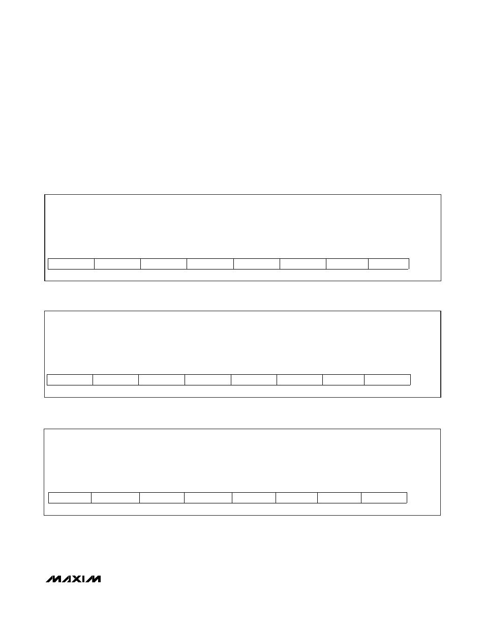
Table 32. ADC Minimum Voltage Conversion Register Format (High-Order Bits)
Description:
Minimum voltage conversion result, high-order bits [9:2]
Register Titles:
min_ch1_mon_h
min_ch2_mon_h
min_ch3_mon_h
min_ch4_mon_h
Register Addresses:
0x14
0x1C
0x24
0x2C
R/W
R/W
R/W
R/W
R/W
R/W
R/W
R/W
RESET
VALUE
vmin_9
vmin_8
vmin_7
vmin_6
vmin_5
vmin_4
vmin_3
vmin_2
0xFF
bit 7
bit 6
bit 5
bit 4
bit 3
bit 2
bit 1
bit 0
Table 33. ADC Minimum Voltage Conversion Register Format (Low-Order Bits)
Description:
Minimum voltage conversion result, low-order bits [1:0]
Register Titles:
min_ch1_mon_l
min_ch2_mon_l
min_ch3_mon_l
min_ch4_mon_l
Register Addresses:
0x15
0x1D
0x25
0x2D
R/W
R/W
R/W
R/W
R/W
R/W
R/W
R/W
RESET
VALUE
vmin_1
vmin_0
0x03
bit 7
bit 6
bit 5
bit 4
bit 3
bit 2
bit 1
bit 0
Table 34. ADC Maximum Voltage Conversion Register Format (High-Order Bits)
Description:
Maximum voltage conversion result, high-order bits [9:2]
Register Titles:
max_ch1_mon_h
max_ch2_mon_h
max_ch3_mon_h
max_ch4_mon_h
Register Addresses:
0x16
0x1E
0x26
0x2E
R/W
R/W
R/W
R/W
R/W
R/W
R/W
R/W
RESET
VALUE
vmax_9
vmax_8
vmax_7
vmax_6
vmax_5
vmax_4
vmax_3
vmax_2
0x00
bit 7
bit 6
bit 5
bit 4
bit 3
bit 2
bit 1
bit 0