Table 41. circular buffer read addresses, Table 42. circular buffer control register format – Rainbow Electronics MAX5961 User Manual
Page 34
MAX5961
0 to 16V, Quad, Hot-Swap Controller
with 10-Bit Current and Voltage Monitor
34
______________________________________________________________________________________
Circular Buffer
The MAX5961 features eight 10-bit circular buffers (in
volatile memory) that contain a history of the 50 most-
recent voltage and current digital conversion results for
each hot-swap channel. These circular buffers can be
read back through the I
2
C interface. The recording of
new data to the buffer for a given signal is stopped
under any of the following conditions:
• The corresponding channel is shut down because of
a fault condition
• A read of the circular buffer base address is per-
formed through the I
2
C interface
• The corresponding channel is turned off by a combi-
nation of the Chx_EN1, Chx_EN2, or ON_ signals
The buffers allow the user to recall the voltage and cur-
rent waveforms for analysis and troubleshooting. The
buffer contents are accessed through the I
2
C interface
at eight fixed addresses in the MAX5961 register
address space (see Table 41).
Each of the eight buffers can also be stopped under
user control by register cbuf_chx_store (see Table 42).
The contents of a buffer can be retrieved as a block
read of either 50 10-bit values (spanning 2 bytes each)
or of 50 high-order bytes, depending on the per-signal
bit settings of register cbufrd_hibyonly (see Table 43).
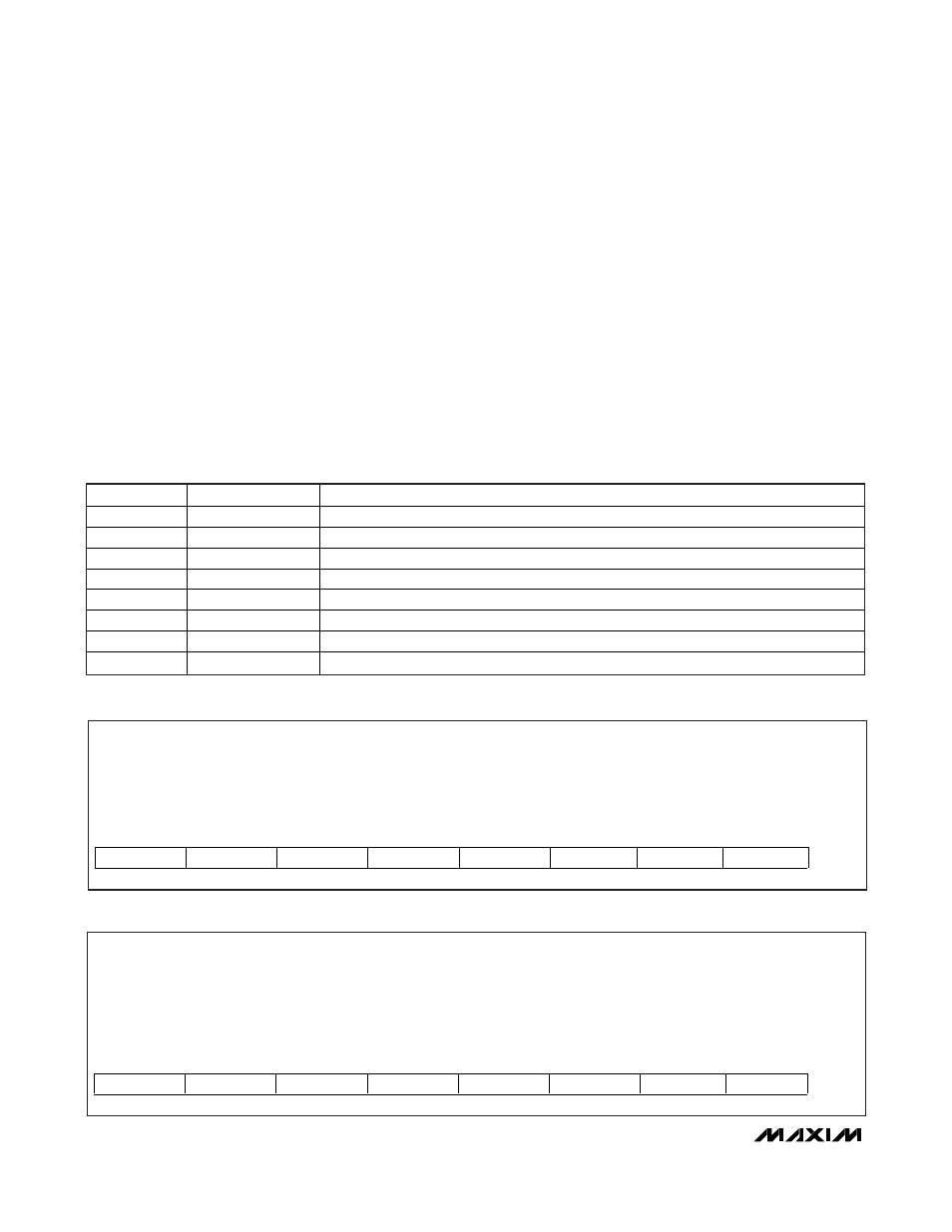
Table 41. Circular Buffer Read Addresses
ADDRESS
NAME
DESCRIPTION
0x80
cbuf_ba_ch1_v
Base address for channel 1 voltage buffer block read
0x81
cbuf_ba_ch1_i
Base address for channel 1 current buffer block read
0x82
cbuf_ba_ch2_v
Base address for channel 2 voltage buffer block read
0x83
cbuf_ba_ch2_i
Base address for channel 2 current buffer block read
0x84
cbuf_ba_ch3_v
Base address for channel 3 voltage buffer block read
0x85
cbuf_ba_ch3_i
Base address for channel 3 current buffer block read
0x86
cbuf_ba_ch4_v
Base address for channel 4 voltage buffer block read
0x87
cbuf_ba_ch4_i
Base address for channel 4 current buffer block read
Table 42. Circular Buffer Control Register Format
Description:
Circular buffer run-stop control register (per-buffer control: 1 = run, 0 = stop)
Register Title:
cbuf_chx_store
Register Address:
0x31
R/W
R/W
R/W
R/W
R/W
R/W
R/W
R/W
RESET
VALUE
ch4_i_run
ch4_v_run
ch3_i_run
ch3_v_run
ch2_i_run
ch2_v_run
ch1_i_run
ch1_v_run
0xFF
bit 7
bit 6
bit 5
bit 4
bit 3
bit 2
bit 1
bit 0
Table 43. Circular Buffer Resolution Register Format
Description:
Circular buffer read-out resolution: high-order byte only, or 8-2 split 10-bit data
(per-buffer control: 1 = high-order byte output, 0 = full-resolution 10-bit output)
Register Title:
cbufrd_hibyonly
Register Address:
0x6D
R/W
R/W
R/W
R/W
R/W
R/W
R/W
R/W
RESET
VALUE
ch4_i_res
ch4_v_res
ch3_i_res
ch3_v_res
ch2_i_res
ch2_v_res
ch1_i_res
ch1_v_res
0x00
bit 7
bit 6
bit 5
bit 4
bit 3
bit 2
bit 1
bit 0