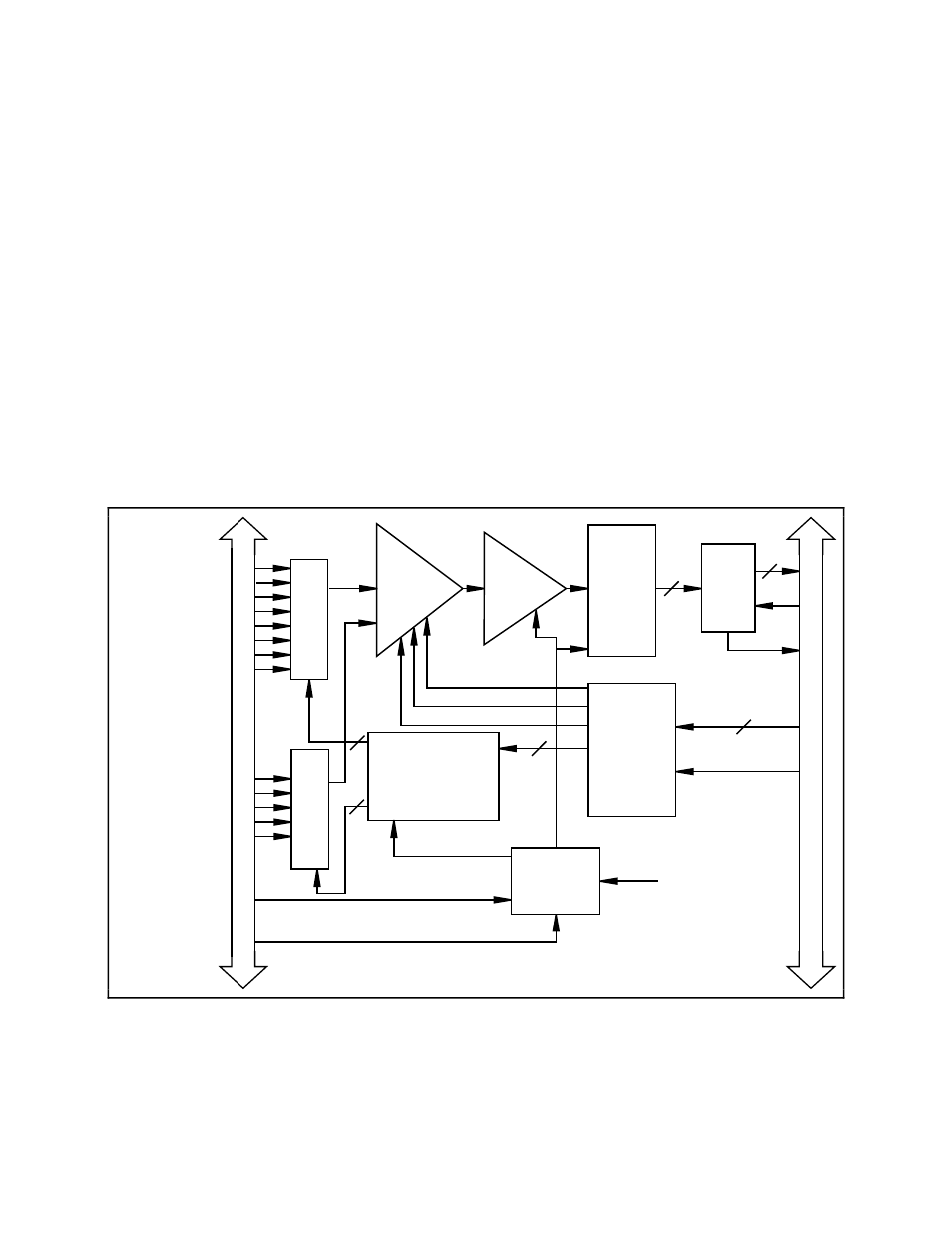
Analog input and data acquisition circuitry, Figure 4-3 – National Instruments Low-Cost Multifunction I/O Board for ISA Lab-PC+ User Manual
Page 63

Theory of Operation
Chapter 4
Lab-PC+ User Manual
4-4
© National Instruments Corporation
•
When a digital I/O port is ready to transfer data
•
When a rising edge signal is detected on Counter A2 output or on the EXTUPDATE line
Each one of these interrupts is individually enabled and cleared.
The DMA control circuitry generates DMA requests whenever an A/D conversion result is
available from FIFO, if the DMA transfer is enabled. The Lab-PC+ supports 8-bit DMA
transfers. DMA Channels 1, 2, and 3 of the PC I/O channel are available for such transfers.
Analog Input and Data Acquisition Circuitry
The Lab-PC+ provides eight channels of analog input with software-programmable gain and
12-bit A/D conversion. Using the timing circuitry, the Lab-PC+ can also automatically time
multiple A/D conversions. Figure 4-3 shows a block diagram of the analog input and data
acquisition circuitry.
Sample-
and-Hold
Amp
PC I/O Channel
Mux
Counter
Data
Acquisition
Timing
Command
Registers
Mux
Pro-
grammable
Gain Amp
ADC
A/D
FIFO
MUX CTR CLK
External Trigger
Counter/Timer
Signals
ADC WR
CONV
AVAIL
A/D
RD
EXT
CONV*
EXT
TRIG
ACH0
ACH1
ACH2
ACH3
ACH4
ACH5
ACH6
ACH7
12
12
8
3
4
A/D
Data
Data
Data
MUX
OUT
I/O Connector
GAIN0
GAIN1
GAIN2
Convert
Mux
3
ACH1
ACH3
ACH5
ACH7
AISENSE/AIGND
Figure 4-3. Analog Input and Data Acquisition Circuitry Block Diagram
