Command register 2 – National Instruments Low-Cost Multifunction I/O Board for ISA Lab-PC+ User Manual
Page 125

Appendix D
Register Map and Descriptions
© National Instruments Corporation
D-9
Lab-PC+ User Manual
Command Register 2
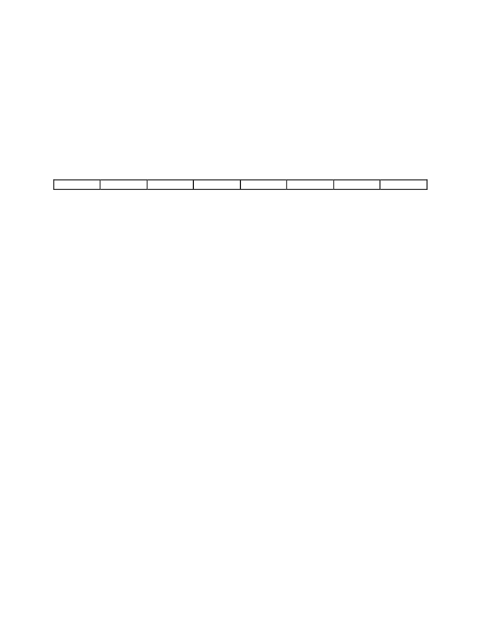
Command Register 2 contains eight bits that control Lab-PC+ analog input trigger modes and
analog output modes.
Address:
Base address + 01 (hex)
Type:
Write-only
Word Size:
8-bit
Bit Map:
7
6
5
4
3
2
1
0
LDAC1
LDAC0
2SDAC1
2SDAC0
TBSEL
SWTRIG
HWTRIG
PRETRIG
Bit
Name
Description
7
LDAC1
This bit is used to enable timer waveform generation from DAC1.
If this bit is set, DAC1 updates its output at regular intervals as
determined by Counter A2 or the EXTUPDATE* signal at the I/O
connector. If this bit is cleared, then the voltage output of DAC1 is
updated as soon as the data is loaded into its data register.
6
LDAC0
This bit is used to enable timer waveform generation from DAC0.
If this bit is set, DAC0 updates its output at regular intervals as
determined by Counter A2 or the EXTUPDATE* signal at the I/O
connector. If this bit is cleared, then the voltage output of DAC0 is
updated as soon as the data is loaded into its data register.
5
2SDAC1
This bit selects the binary coding scheme used for the DAC1 data.
If this bit is set, a two's complement binary coding scheme is used
for interpreting the 12-bit data. Two's complement is useful if a
bipolar output range is selected. If this bit is cleared, a straight
binary coding scheme is used. Straight binary is useful if a
unipolar output range is selected.
4
2SDAC0
This bit selects the binary coding scheme used for the DAC0 data.
If this bit is set, a two's complement binary coding scheme is used
for interpreting the 12-bit data. Two's complement is useful if a
bipolar output range is selected. If this bit is cleared, a straight
binary coding scheme is used. Straight binary is useful if a
unipolar output range is selected.
3
TBSEL
This bit is used to select the clock source for A/D conversions. If
this bit is cleared, an internal 1 MHz clock drives the counter
(Counter A0), and the interval between samples is the value loaded
into Counter A0 multiplied by 1
µ
s. If this bit is set, then the
output of user-programmable Counter B0 is used as a clock source.
The timebase for Counter B0 is fixed at 2 MHz and cannot be
changed. The interval between acquired samples is the value
loaded into Counter A0 multiplied by the period of the output
signal from Counter B0.
