3 programming the j1850 delay compensation (j – Intel 8XC196Lx User Manual
Page 85
8-19
J1850 COMMUNICATIONS CONTROLLER
8.6.3
Programming the J1850 Delay Compensation (J_DLY) Register
The J1850 delay compensation register (Figure 8-18) allows you to program the necessary delay
time through the external transceiver to compensate for the inherent propagation delays and to
accurately resolve bus contention during arbitration.
2
—
Reserved; for compatibility with future devices, write zero to this bit.
1:0
PRE1:0
J1850 Oscillator Prescaler
These bits ensure proper operation of the J1850 peripheral at the supported
input frequencies (F
XTAL
1
).
PRE1
PRE0
F
XTAL
1
0
0
8 MHz
0
1
12 MHz
1
0
16 MHz
1
1
20 MHz
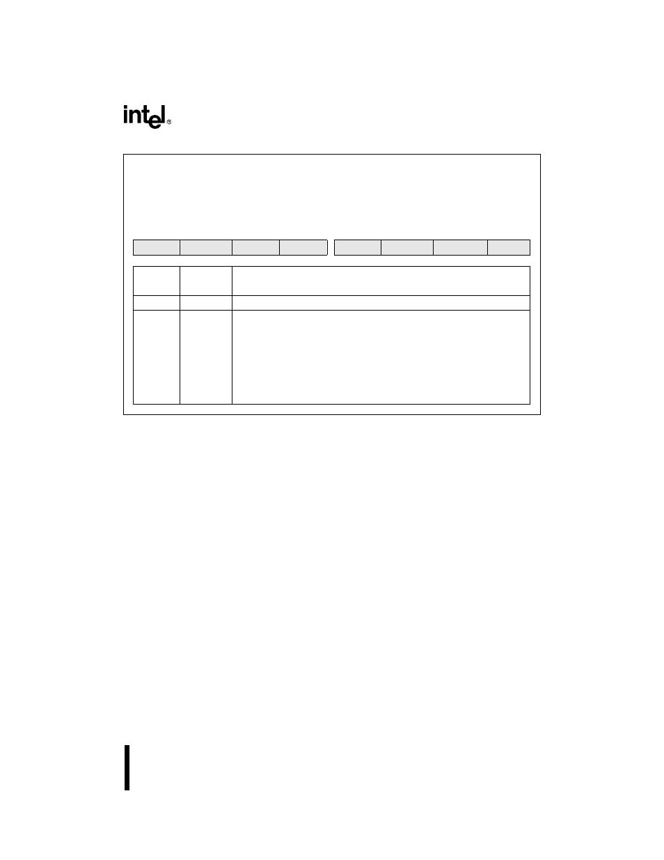
J_CFG
Address:
Reset State:
1F54H
00H
The J1850 configuration (J_CFG) register selects the proper oscilator prescaler, initiates transmission
break for debug, invokes clock quadrupling operation, and selects the normalizartion bit format. This
byte register can be directly addressed through
windowing. All J1850 bus activity is ignored until you
first write to this register.
7
0
NBF
IFR3
4XM
TXBRK
RXPOL
—
PRE1
PRE0
Bit
Number
Bit
Mnemonic
Function
Figure 8-17. J1850 Configuration (J_CFG) Register (Continued)