2 functional description, 1 module overview, The following shows a block diagram of the smt321 – Sundance SMT321 User Manual
Page 8
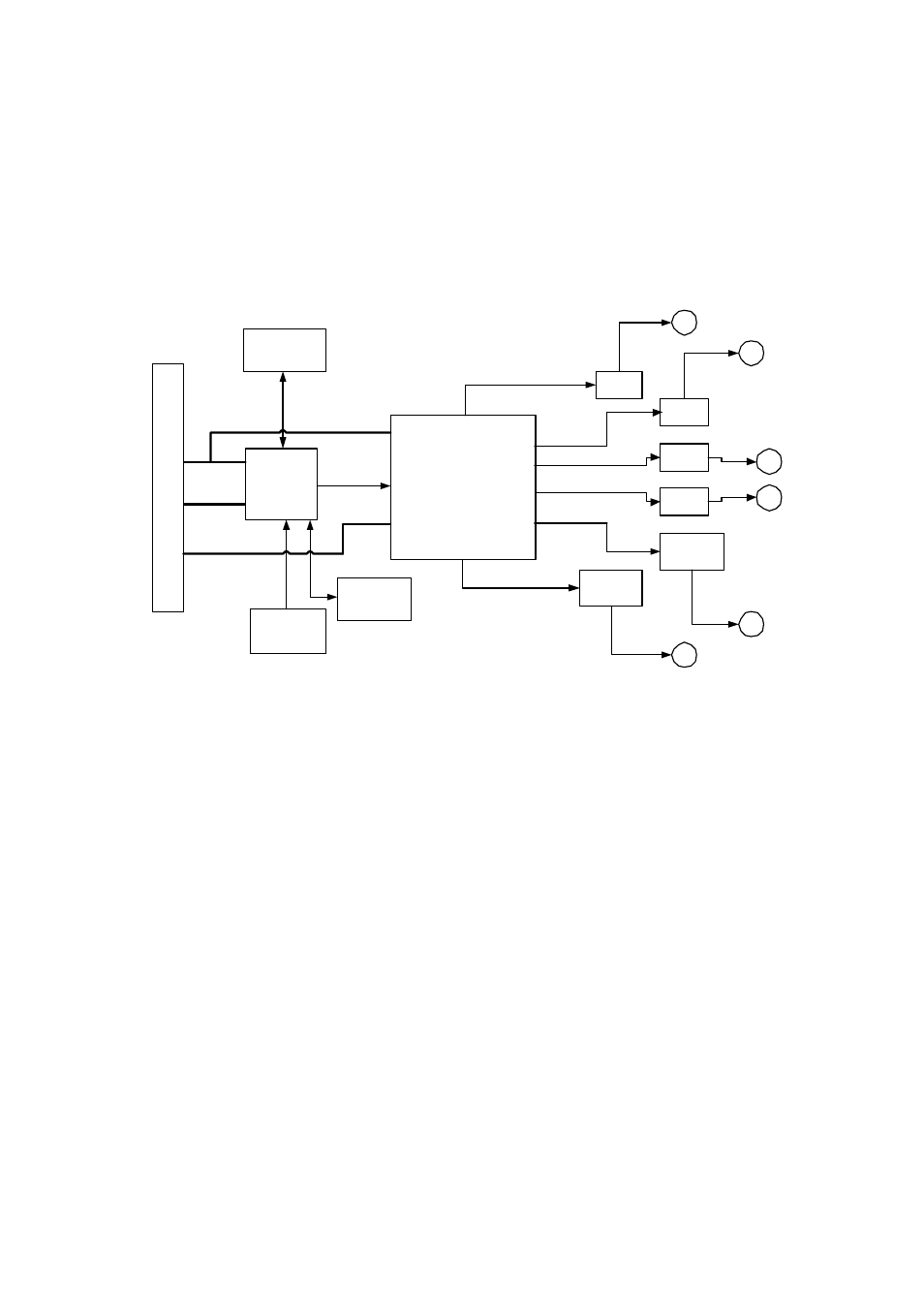
2 Functional Description
2.1 Module Overview
The following shows a block diagram of the SMT321.
TTL to
LVPECL
TTL to
LVPECL
LVPECL
Clock
Generation
VCO
VCO
LVPECL
Clock
Generation
Xilinx Spartan 3 FPGA
(XC3S400 - TQ144)
Trigger
Connector
Trigger
Connector
Analog
Connector
Analog
Connector
Clock
Connector
Clock
Connector
Texas Inst
MSP430F149
T
I
M
C
o
n
n
e
c
t
o
r
Temprature
Sensor
Voltages from
board
Serial number
Comport 3
Comport 0
Control
Signals
Config
Figure 1.Functional Block Diagram of the SMT321.
The user sets up the triggers, analog and clock signals in the FPGA via the comports
using a software interface on the Personal Computer. This sets up the internal registers
of the firmware design.
The triggers are generated by the FPGA itself. It scales a 10MHz clock by using two
counters, one for the high time of the trigger and one for the low time of the trigger. Thus
the maximum frequency attainable by the triggers is 5MHz.
The analog signals are generated by generating a variable voltage on the VCO using a
1024 position digital potentiometer. Using the FPGA to program the potentiometer to a
certain voltage the VCO’s swings to new frequencies depending on the voltage applied
to them.
Finally the clocks are generated by clock synthesizers. The synthesizers are
programmed to a certain frequency using the FPGA.