8 analog signal output – Sundance SMT321 User Manual
Page 15
attainable at the system clock of 10MHz. From here the trigger can be shaped into any
shape as the high and low time are independent of each other.
If the one pulse is activated (and the multiplexer selects the one pulse module) it pulses
the channel with one pulse of a width determined by the pulse high register. If the pulse
high register is set up for one it will pull the channel high for one clock (system clock)
and pull it low indefinitely. In order for another pulse to be generated the pulse module
must receive an enable signal which will once again send a pulse down the channel with
a width depending on the register value.
The two channels are totally independent and thus can be used in this fashion. For
example having a pulse activated on Channel A with a width of 30 clocks and a
continuous trigger on Channel B with a high time of 2 clocks and a low time of 10 clocks.
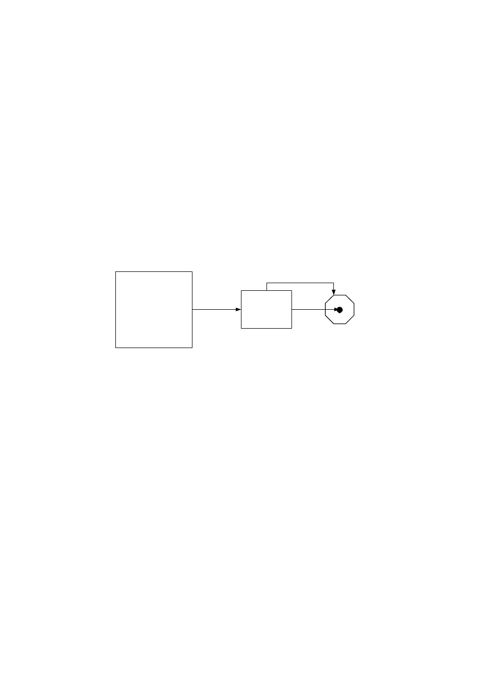
The trigger outputs are LVPECL. A diagram of the trigger path from the FPGA is shown
in figure 5.
FPGA
TTL to
LVPECL
+ve
-ve
No ground on
connector
Figure 5. Trigger path from FPGA to output.
2.8 Analog Signal Output
As shown in Table 1 the analog signal which is generated in the two analog channels
depends on the VCO present in the channel. The VCO’s are switched by the digital pod
which has two outputs for both VCO’s present on the board. The digital pod can swing
from 0 Volt to 18Volts, but the VCO’s only works from 1 Volt to 16 Volts (High frequency
boards works from 1 Volt – 12 and 15 Volts) which gives a decrease in the pod’s
resolution.
Depending on the VCO model and voltage applied to the VCO an analog signal can be
generated in each channel independent of each other. Figure 6 shows the analog signal
path from the FPGA.