3 data stream description, 1 description of internal fpga blocks – Sundance SMT321 User Manual
Page 10
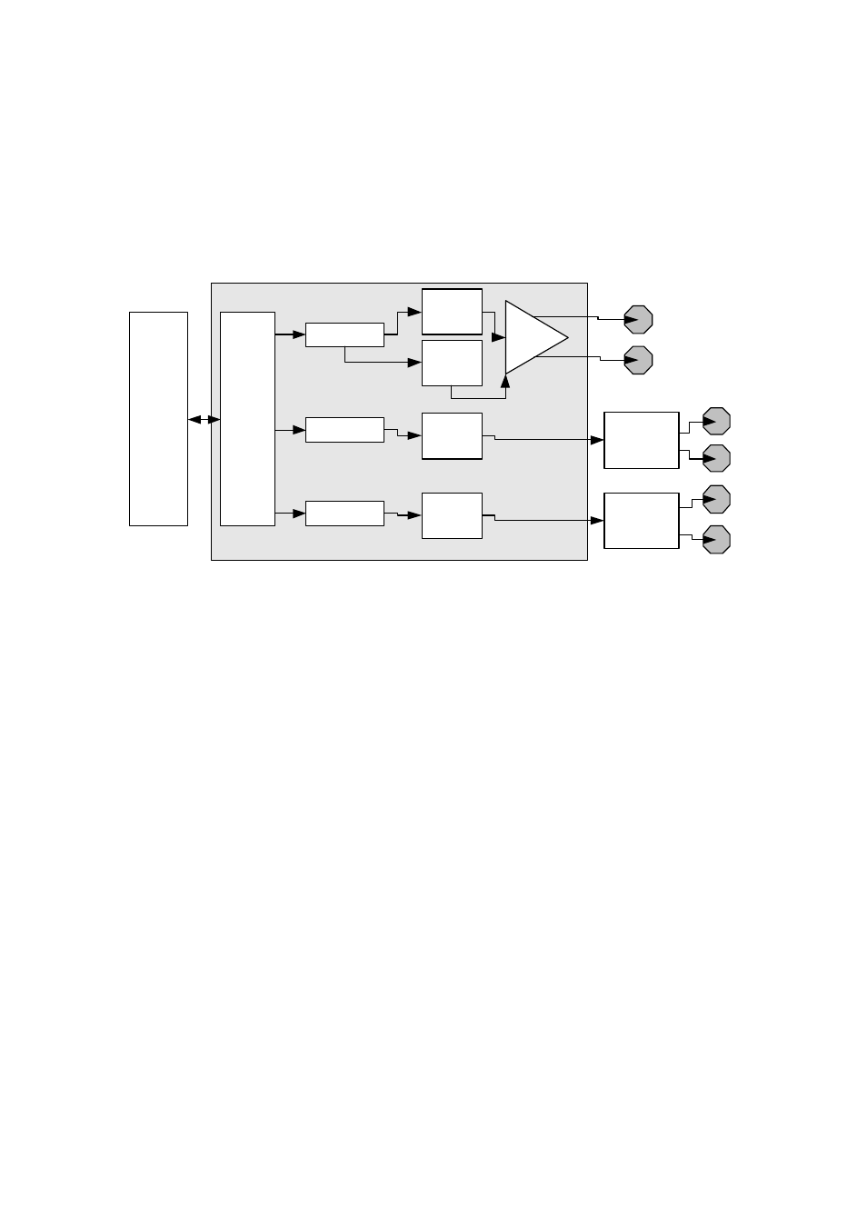
2.3 Data Stream Description
The module and the FPGA have three different data paths depending on the output.
Each architecture has two separate channels for a total of six outputs on the SMT321.
The following figure illustrates the data path of the FPGA and module.
Comport
Comport
Decoding
Trigger
Registers
Digital Pod
Registers
Clock
Registers
Trigger
Setup x 2
Trigger
Pulse
Setup x 2
Mux x2
Digital Pod
Setup
Clock
Setup x2
VCO x2
Clock
Sy nehsizer x2
Output
Output
Output
Output
Output
Output
FPGA
Figure 2. Data path of the FPGA and module.
The user configures the SMT321 via the comport decoding block in firmware. All the
registers needed for the generation of the test signals is configured by the decoding
block and then all the setup blocks are enabled. Once the setup blocks are enabled the
registers values are clocked into the different blocks which activates the different signals.
If a change in any channel is desired the user sends the change to the specific register
and enables the activate pulse on the specific channel. The new register value will be
clocked into the specific setup block and the chosen signal will change accordingly.
2.3.1 Description of Internal FPGA Blocks
Comport Decoding
This block receives the module setting made by the user via the DSP interface using the
PC. It then decodes the data and configures the specific registers.
Trigger Registers, Trigger Setup, Trigger Pulse Setup and Multiplexer
The trigger setup consist of six 16-bits registers, three enable signals and two
multiplexer signals. The last two signals are needed to select between a continuous
trigger and a single pulse on each channel.