4 register descriptions, 1 com in scratch registers, 2 clock control registers – Sundance SMT321 User Manual
Page 24
0x026
Trigger Pulse Multiplexer Channel A
Reserved
0x027
Trigger Pulse Multiplexer Channel B
Reserved
.
Reserved
Reserved
.
Reserved
Reserved
0x030
Digital Pod Register MSB
Reserved
0x031
Digital Pod Register LSB
Reserved
.
Reserved
Reserved
.
Reserved
Reserved
0x040
Digital IOS output register
Reserved
Table 5. Register Memory Map.
4.4 Register Descriptions
4.4.1 Com In Scratch Registers
Any value or data can be written to these 16bit registers. These registers are more for
debugging purposes and have no influence in the firmware design.
4.4.2 Clock Control Registers
These registers are used in the setup of the clock outputs of the SMT321. The table
below shows the setup of the registers:
Clock Control Register
Byte
Bit 7
Bit 6
Bit 5
Bit 4
Bit 3
Bit 2
Bit 1
Bit 0
0
NO CARES
Test Bits
Output Division
M Count
1
M Count
Table 6. Clock Control setup registers.
As the comport bit stream is 16 bits long both bytes are written simultaneously. The most
significant byte (Byte 0) contains the test bits, output division bits and one M count bit.
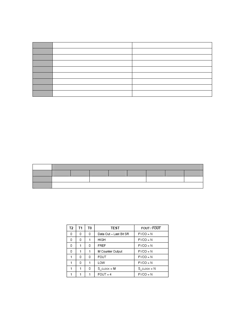
The test bits selects between various internal node values and is controlled by the T[2:0]
bits in the serial data stream. The node values are shown in table 7.
Table 7. Test bit configurations.