9 clock output, 10 connectors pin outs – Sundance SMT321 User Manual
Page 16
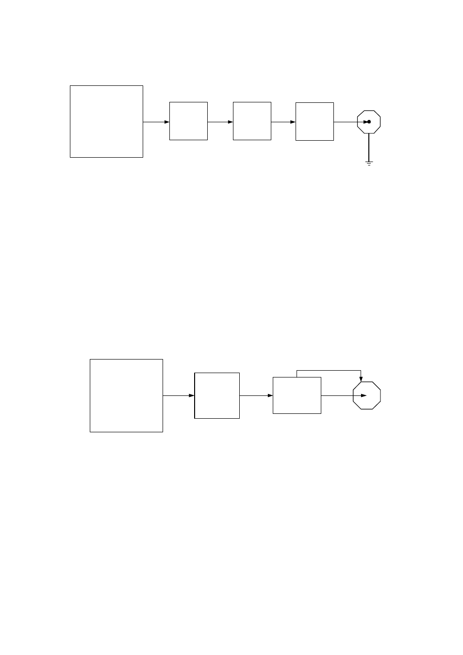
FPGA
Digital
Pod
VCO
Attenuator
10dBm
Control
Voltage
Connector
GND
10dBm (typ)
Analog signal
0dBm
output
Figure 6. Analog signal path from FPGA to output.
2.9 Clock Output
The two channels implemented by the clock signals each have its own setup register
which contains a 14bit configuration word. The clocks are generated by the two clock
synthesizers present on the board. And the output is LVPECL.
The user configures the registers via the comports and the resulting clock is then
achieved. When the user writes to the registers the firmware module is automatically
updated and thus the clock.
Each channel can have a different clock running in them as there are two synthesizers
and thus two different clocks. Figure 7 shows the clock path from the FPGA to the
output.
FPGA
TTL to
LVPECL
+ve
-ve
No ground
on connector
Clock
Synthesizer
Figure 7. Clock path from FPGA to output.
2.10 Connectors Pin outs
Figure 8 shows all the connectors on SMT321. Each connector’s pin outs will be
discussed in the following subsections.