Sundance SMT391-VP User Manual
Page 36
Version 1.3
Page 36 of 41
SMT391-VP User Manual
The Clock Synthesizer register (present on the SMT338-VP firmware side) is used for
the setup of the clock synthesizer on the SMT391. The table below shows the setup
of this register:
Clock Control Register
Byte
Bit 7
Bit 6
Bit 5
Bit 4
Bit 3
Bit 2
Bit 1
Bit 0
1
Do Not Care
Test Bits
Output Division
M Count
0
M Count
Figure 24 – Clock Synthesizer Register.
As the Comport bit-stream is 16 bits long both bytes are written simultaneously. The
most significant byte (Byte 1) contains the test bits, output division bits and one M
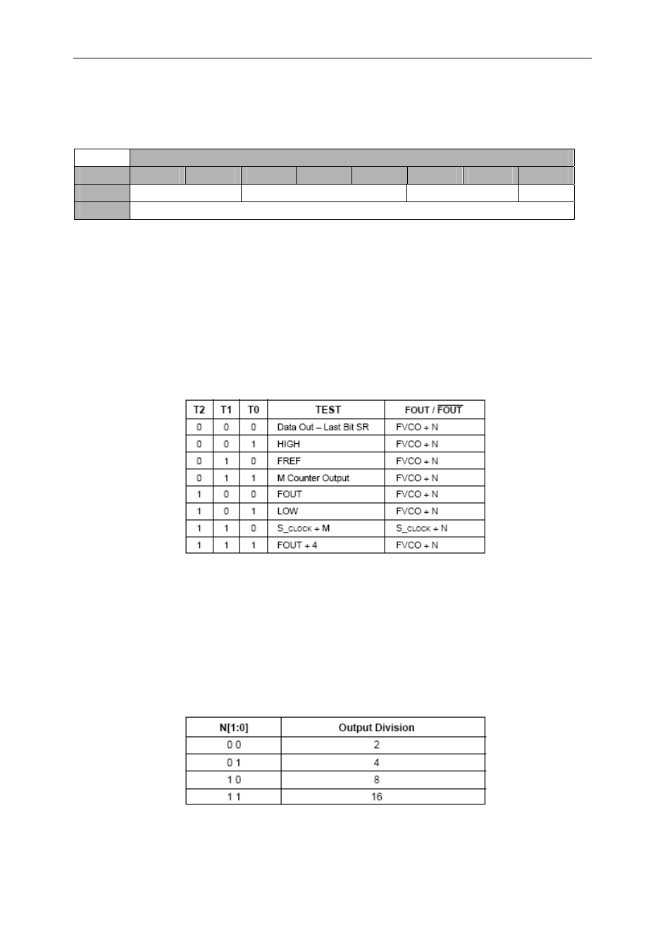
count bit. The test bits selects between various internal node values and is controlled
by the T[2:0] bits in the serial data stream (This feature is can be set up by the
FPGA, but the value of the Test output is not read by the FPGA). The node values
are shown in the table below.
Figure 25 – Clock Synthesizer Test Output.
Output division on the clock synthesizer is achieved by the two output division bits
found in the first byte of the clock control register. These configurations are
underneath: