Sundance SMT391-VP User Manual
Page 26
Version 1.3
Page 26 of 41
SMT391-VP User Manual
0x2
0x2
0x2
0x2
0x022
0x023
0x024
0x025
SMT338-VP Serial No
SMT338-VP Serial No
SMT338-VP Serial No
SMT338-VP Serial No
Byte A
Byte B
Byte C
Byte D
0x2
0x2
0x2
0x2
0x02A
0x02B
0x02C
0x02D
SMT391 Serial No
SMT391 Serial No
SMT391 Serial No
SMT391 Serial No
Byte A
Byte B
Byte C
Byte D
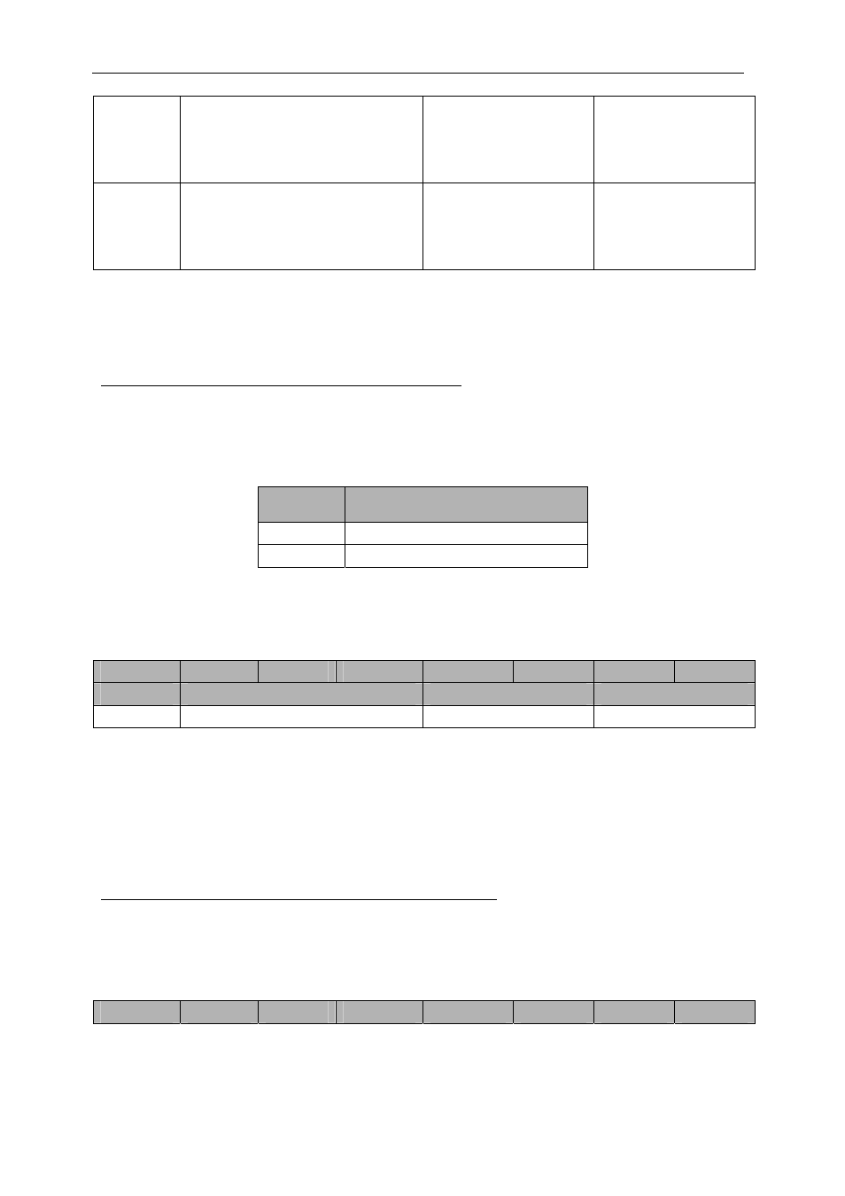
Figure 10 – Serial Number Registers Cont. (Read Only).
ADC Clock Source Registers (Write Add 0x801)
The ADC can receive a clock from the on-board VCO or the on-board clock
synthesizer. The following table shows the different combinations for setting up the
SMT391 clock tree.
Register
Value
ADC Clock Source
0x0000 On-board
VCO
0x0001 On-board
Clock
Synthesizer
Figure 11 – Clock Source Selection Table (Write Only).
31 .. 28
27 .. 24
23 .. 20
19 .. 16
15 .. 12
11 .. 8
7 .. 4
3 .. 0
Command
Address
Data MSB
Data LSB
0x1
0x801
0x00
Clock Register Value
Figure 12 – Clock Source Register (Write Only).
Clock Synthesizer Setup Register (Write Add 0x800)
This register sets up the frequency of the clock synthesizer on the SMT391. Any write
operation to this register will trigger the clock synthesizer interface control logic to
initialize the clock synthesizer with its new value.
31 .. 28
27 .. 24
23 .. 20
19 .. 16
15 .. 12
11 .. 8
7 .. 4
3 .. 0