Firmware – Sundance SMT391-VP User Manual
Page 11
Version 1.3
Page 11 of 41
SMT391-VP User Manual
Clocks generation
The sampling clock of the ADC can be generated by an on-board VCO or an on-
board clock synthesiser. Inputs for external clocks are available on the board but not
supported by the FPGA design.
Refer to the SMT391 user manual for further information.
Firmware
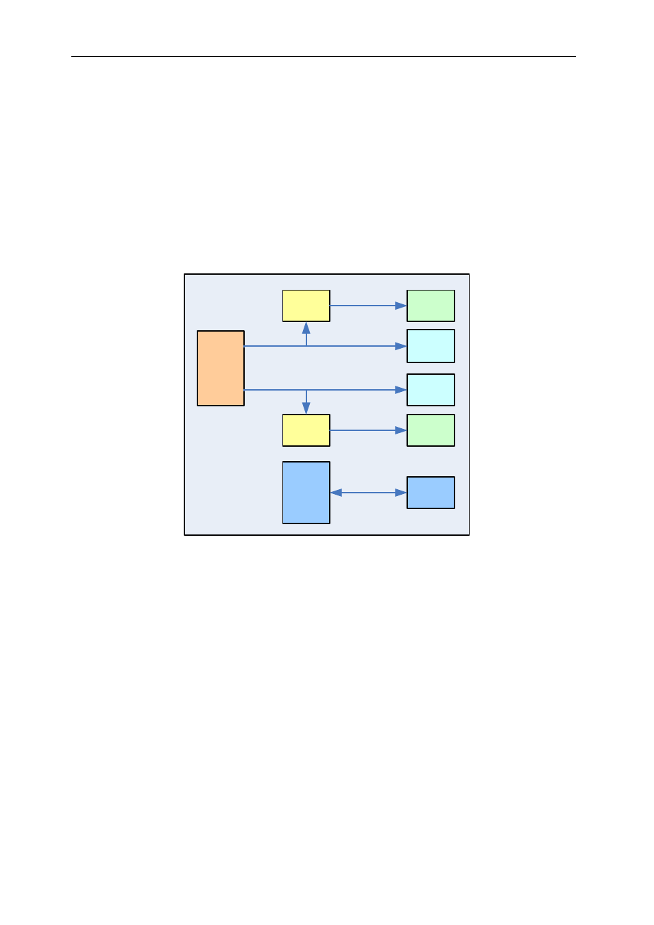
Block diagram
The following diagram represents the internal architecture of the FPGA of the
SMT391-VP.
SMT391
interface
block
Buffer
SDB
RSL
Registers
Comport
SDB
RSL
Buffer
64 bits
64 bits
SMT391 interface block
The following diagram shows the various blocks constituting the SMT391 block.
The SMT391 interface block implements the interface to the SMT391 daughter
module.
It receives the 1Gsps data stream coming from the ADC and provides it to the rest of
the design.
The data sampled by the ADC are output by this block, 8 samples at a time (64 bits)
at a 1/8 of the sampling clock of the ADC.
The firmware of the SMT391-VP supports one clock input for the ADC.
The ADC must be configured using the following clock selection mode:
-
CLKI
Æ
ADCI