Sundance SMT391-VP User Manual
Page 23
Version 1.3
Page 23 of 41
SMT391-VP User Manual
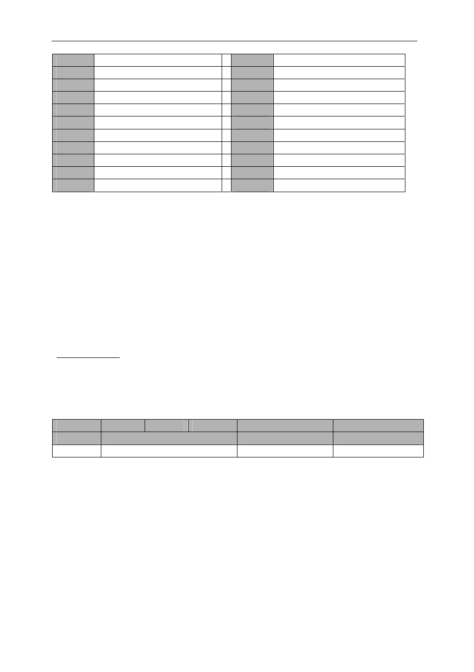
0x805
Smt391Pll_IfN_Reg2
0x805
Reserved
0x806
Smt391Pll_RfR_Reg1
0x806
Reserved
0x807
Smt391Pll_RfR_Reg2
0x807
Reserved
0x808
Smt391Pll_RfN_Reg1
0x808
Reserved
0x809
Smt391Pll_RfN_Reg2 *
0x809
Reserved
0x80A
Smt391AdcCntrlReg
0x80A
Reserved
0x80B
Smt391AdcCntrlAddress
0x80B
Reserved
0x80C
Smt391AdcCntrlData *
0x80C
Reserved
0x80D
Reserved
0x80D
Reserved
0x80E
Reserved
0x80E
Reserved
0x80F
Reserved
0x80F
Reserved
* Write Data Valid pulse is generated when this register is written to.
+ A pre-read is generated on the first read. A second read is required to read the real
data.
Figure 5 – Register Memory Map.
For registers larger than 16 bits with an LSB and MSB part always write the LSB part
first and then the MSB.
Register Descriptions
Reset Register
The reset register is used to reset the various blocks constituting the FPGA.
Writing a ‘1’ will put the selected block in the reset state. Writing a ‘0’ will release the
reset.
31 .. 28
27 .. 24
23 .. 20
19 .. 16
15 .. 9
8 .. 0
Command
Address
Data MSB
Data LSB
1 0x000
Reserved
Reset
command
Figure 6 – Reset Register (Write Only).
Reset command:
Bit 0: global reset of the FPGA. Reset all the logic in the FPGA except the comport
and the register block.
Bit 1: ADC interface channel Q reset (do not use).
Bit 2: ADC interface channel I reset.
Bit 3: SDB A reset.