Sundance SMT391-VP User Manual
Page 14
Version 1.3
Page 14 of 41
SMT391-VP User Manual
Registers block
This block implements the registers of the SMT391-VP. The complete description of
the registers is available in the section “Description of the registers”. The registers
are updated via the comport 3 of the SMT391-VP.
The register block can not be reset to its default value. User must set each individual
register to the requested value.
SDB
The SMT391-VP implements two 32-bits SDB interfaces. Refer to the SMT6500 for
the complete description of the SDB.
The SDBs are clocked at 62.5 Mhz.
RSL
The SMT391-VP implements two groups of four RSL. There is one group of four
RSL per ADC channel.
The RSL makes used by default of a 10/8 encoding style which allow a data rate of
125 MB/sec per RSL. The main part of the data sent on the RSL is the ADC data.
However some control command is also part of the data stream, reducing slightly the
data rate below 1 GB/sec.
Comport
The SMT391-VP implements one comport interface.
Only the comport 3 is implemented.
Refer to the SMT6500 for the complete description of the comport.
MPS430 block
The SMT391-VP implements the interface to the micro-controller MPS430. The
FPGA can receive information such as the temperature of the ADC via this interface.
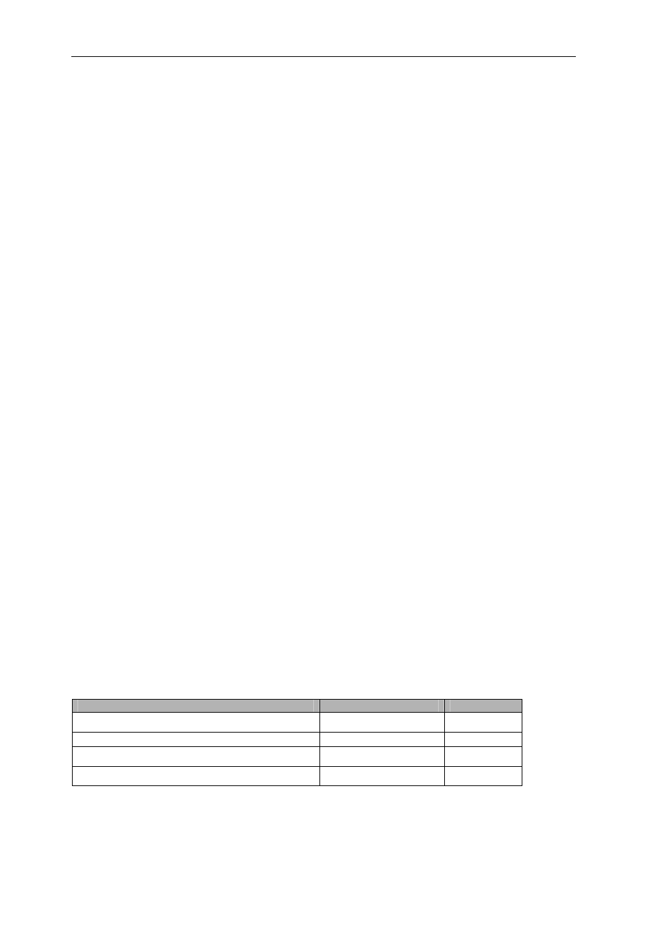
Design Resource Usage
The following table is a summary of the FPGA resources used by the demo design
that comes with the SMT391-VP (compiled for a VP30 device).
Resource
Utilization
Percentage
Number of External DIFFMs
37 out of 276
13%
Number of External DIFFSs
37 out of 276
13%
Number of External IOBs
244 out of 556 47%
Number of LOCed External IOBs 244 out of 244
100%