The data in the registers is arranged as follow – Sundance SMT391-VP User Manual
Page 27
Version 1.3
Page 27 of 41
SMT391-VP User Manual
Command
Address
Data MSB
Data LSB
0x1 0x800
Data Data
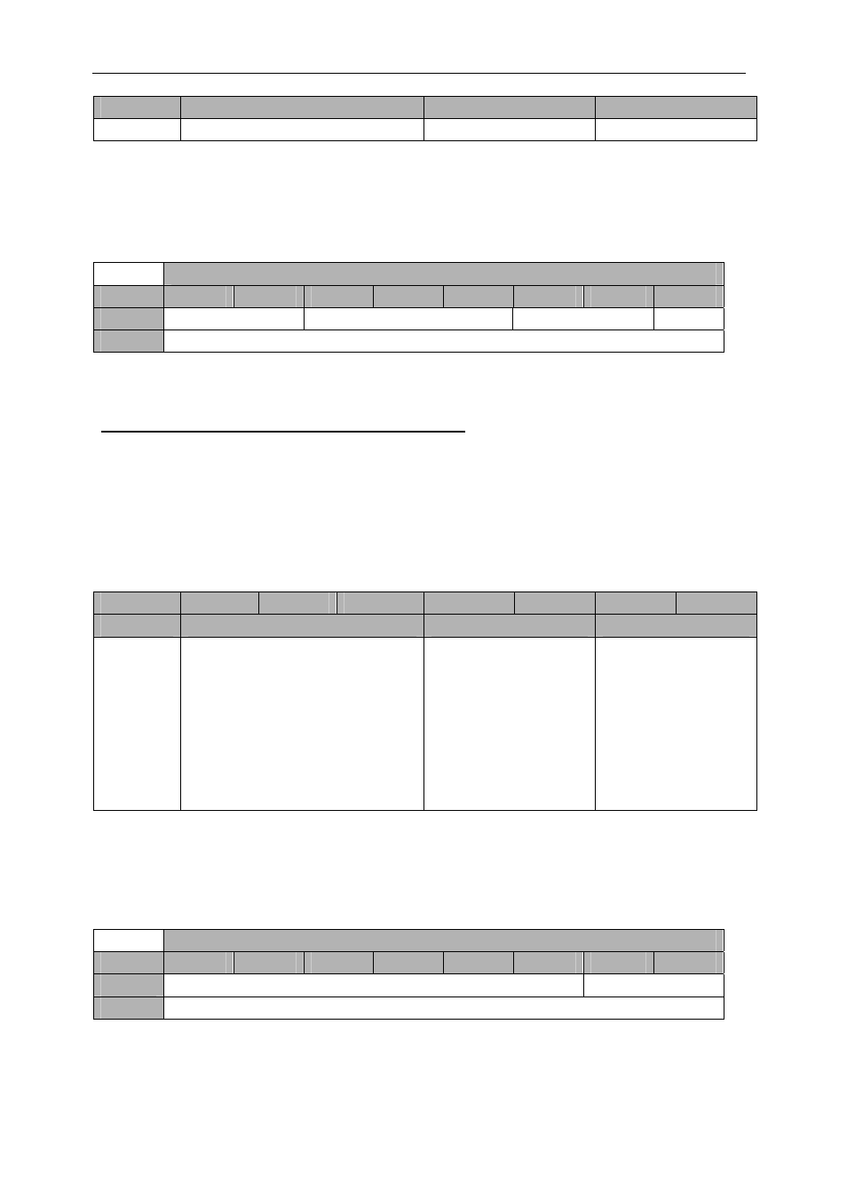
Figure 13 – Clock Synthesizer Setup Register (Write Only).
The data is arranged as follow:
Clock Control Register
Byte
Bit 7
Bit 6
Bit 5
Bit 4
Bit 3
Bit 2
Bit 1
Bit 0
1
Do Not Care
Test Bits
Output Division
M Count
0
M Count
Refer to the appendix for more details.
PLL Setup Registers (Write Add 0x802 – 0x809)
These registers set up the frequency of the PLL circuit on the SMT391. There are
two sets of registers – one set for setting up the IF side of the PLL, and the other set
for setting up the RF side of the PLL. The IF side is connected to a 200 – 350 MHz
VCO circuit and the RF side is connected to a 600 – 1000 MHz VCO circuit. All
registers must be initialized, and only when writing to the final register will both the IF
and RF side be configured to their new values.
31 .. 28
27 .. 24
23 .. 20
19 .. 16
15 .. 12
11 .. 8
7 .. 4
3 .. 0
Command
Address
Data MSB
Data LSB
0x1
0x1
0x1
0x1
0x1
0x1
0x1
0x1
0x802
0x803
0x804
0x805
0x806
0x807
0x808
0x809
Smt391Pll_IfR_Reg1
Smt391Pll_IfR_Reg2
Smt391Pll_IfN_Reg1
Smt391Pll_IfN_Reg2
Smt391Pll_RfR_Reg1
Smt391Pll_RfR_Reg2
Smt391Pll_RfN_Reg1
Smt391Pll_RfN_Reg2
Smt391Pll_IfR_Reg1
Smt391Pll_IfR_Reg2
Smt391Pll_IfN_Reg1
Smt391Pll_IfN_Reg2
Smt391Pll_RfR_Reg1
Smt391Pll_RfR_Reg2
Smt391Pll_RfN_Reg1
Smt391Pll_RfN_Reg2
Figure 14 – PLL Setup Registers (Write Only).
The data in the registers is arranged as follow:
Smt391Pll_IfR_Reg1 - Smt391Pll_RfR_Reg1
Byte
Bit 7
Bit 6
Bit 5
Bit 4
Bit 3
Bit 2
Bit 1
Bit 0
1
R_CNTRL (5 .. 0)
Address field
0
R_CNTRL (13 .. 6)