Analog output – Measurement Computing PCI-DAS6071 User Manual
Page 39
PCI-DAS6071 User's Guide
Specifications
39
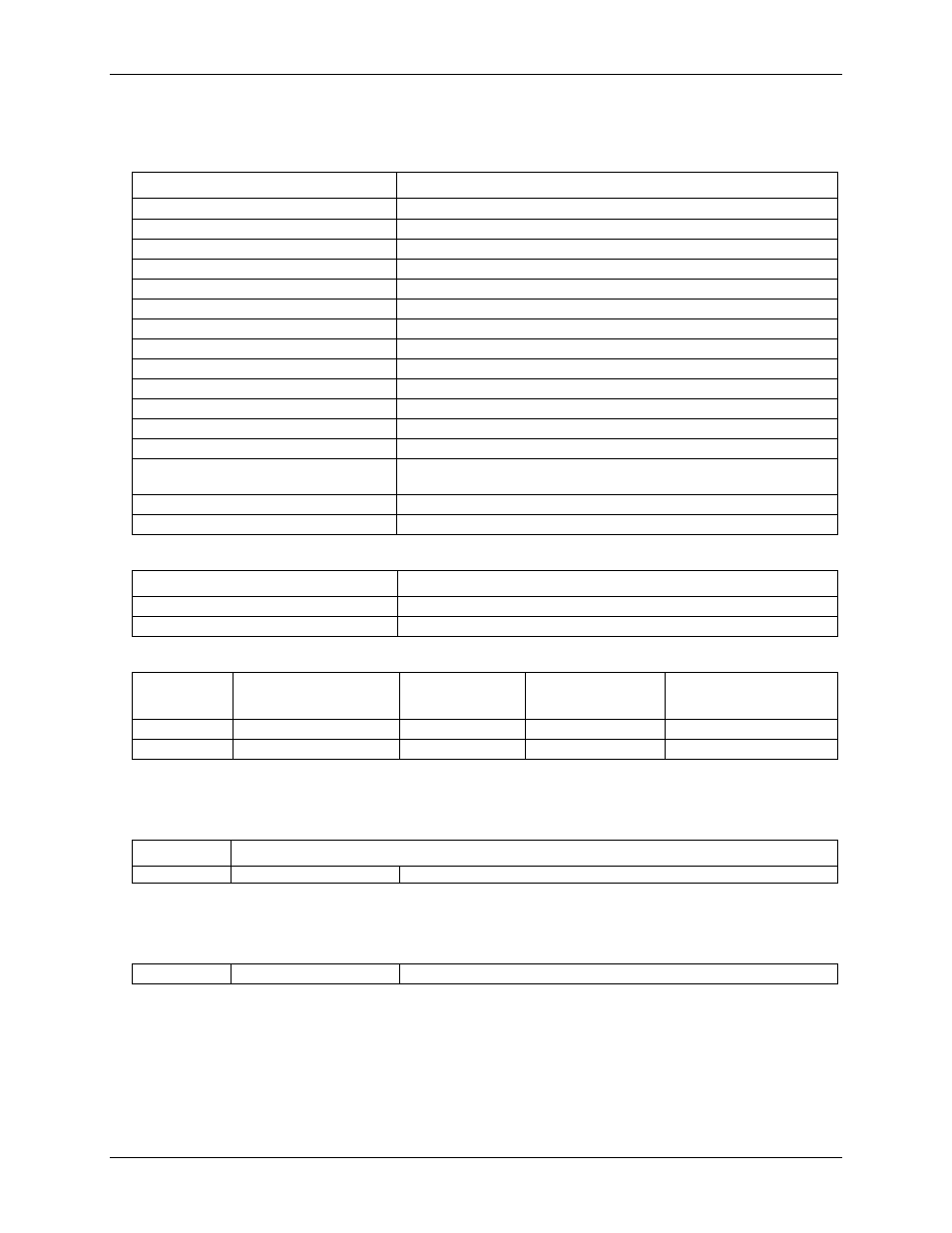
Analog output
Table 9. AO specifications
Parameter
Specification
D/A converter type
Double-buffered, multiplying
Resolution
12-bits, 1-in-4096
Number of channels
2 voltage output
Voltage range
±10 V, 0 to 10 V, ±EXT REF., 0 to EXT REF., software selectable
Monotonicity
12-bits, guaranteed
Slew rate
20 V/µs min
Settling time (full scale step)
3.0 µS to ±0.5 LSB accuracy
Noise
200 µVrms, DC to 1MHz BW
Glitch energy
±20 mV @ 1.5 µS duration measured at mid-scale transition.
Current drive
±5 mA
Output short-circuit duration
Indefinite @ 25 mA
Output coupling
DC
Output impedance
0.1 Ω max
Gain temperature coefficient, internal or
external reference
25 ppm/°C
Offset temperature coefficient
±50 µV/°C
Power up and reset
DACs cleared to 0 volts ±200 mV max
Table 10. Analog output absolute accuracy specifications
Range
Absolute Accuracy (LSB)
±10 V
±1.7 LSB
0 to 10 V
±2.3 LSB
Table 11. Analog output absolute accuracy components specifications
Range
% of Reading
Offset
(mV)
Temp Drift
(%/DegC)
Absolute Accuracy at
FS (mV)
±10 V
±0.0219
±5.93
±0.0005
±8.127
0 to 10 V
±0.0219
±3.49
±0.0005
±5.685
Each PCI-DAS6071 is tested at the factory to assure the board’s overall error does not exceed the limits listed in
Table 10.
Table 12. Relative accuracy specifications
Range
Relative Accuracy
All ranges
±0.3 LSB, typ
±0.5 LSB, max
Relative accuracy is defined as the measured deviation from a straight line drawn between measured endpoints
of the transfer function.
Table 13. Differential non-linearity specifications
All ranges
±0.3 LSB, typ
±1.0 LSB, max