Power, Power –25 – Altera Transceiver Signal Integrity Development Kit, Stratix IV GX Edition User Manual
Page 35
Chapter 2: Board Components
2–25
Power
November 2011
Altera Corporation
Transceiver Signal Integrity Development Kit,
Stratix IV GX Edition Reference Manual
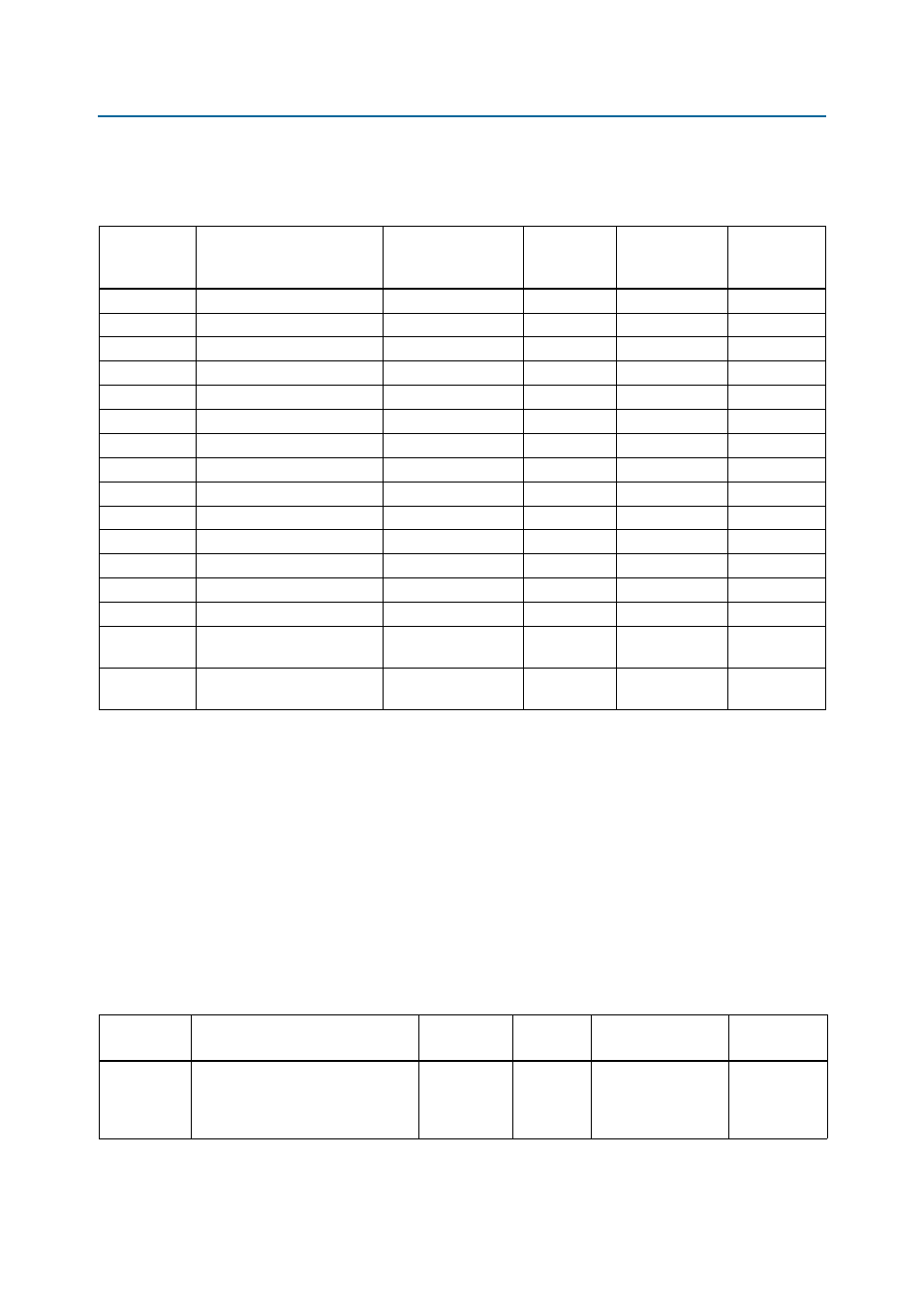
summarizes the transceiver channels available on the Stratix IV GX
transceiver signal integrity development board.
All receive channels include a 0402 type 0.1-µF DC blocking capacitor in series with
the P and N signals to remove the DC component of the transmitted signal. The
receivers internally regenerate the required DC offset. Blocking capacitors are not
provided for the transmit channels.
Power
The board’s power is provided through a laptop style DC power input. The input
voltage must be in the range of 14 V to 20 V. The DC voltage is then stepped down to
the various power rails used by the components on the board.
The slide switch (SW1) is the board power switch.
lists the connection of
this power switch.
Table 2–28. Transceiver Channel Pin-Out
Board
Reference
Description
Schematic Signal
Name
I/O Standard
Stratix IV GX
Device Pin
Number
Other
Connections
J34, J36
Left GXB0 TX Channel
GXB0L_TX0[p/n]
—
AT36, AT37
—
J30, J32
Left GXB0 RX Channel
GXB0L_RX0[p/n]
—
AU38, AU39
—
J39, J41
TX1 from Left GXB1 Block
GXB1L_TX1[p/n]
—
P36, P37
—
J38, J40
RX1 from Left GXB1 Block
GXB1L_RX1[p/n]
—
R38, R39
—
J43, J45
TX2 from Left GXB1 Block
GXB1L_TX2[p/n]
—
T36, T37
—
J42, J44
RX2 from Left GXB1 Block
GXB1L_RX2[p/n]
—
U38, U39
—
J55, J57
TX3 from Left GXB1 Block
GXB1L_TX3[p/n]
—
AB36, AB37
—
J54, J56
RX3 from Left GXB1 Block
GXB1L_RX3[p/n]
—
AC38, AC39
—
J59, J61
TX4 from Left GXB1 Block
GXB1L_TX4[p/n]
—
AD36, AD37
—
J58, J60
RX4 from Left GXB1 Block
GXB1L_RX4[p/n]
—
AE38, AE39
—
J47, J49
TX5 from Left GXB1 Block
GXB1L_TX5[p/n]
—
V36, V37
—
J46, J48
RX5 from Left GXB1 Block
GXB1L_RX5[p/n]
—
W38, W39
—
J51, J53
TX6 from Left GXB1 Block
GXB1L_TX6[p/n]
—
Y36, Y37
—
J50, J52
RX6 from Left GXB1 Block
GXB1L_RX6[p/n]
—
AA38, AA39
—
J31, J33
33 in. long transmitter
channel from Left GXB2 Block
GXB2L_TX7[p/n]
—
B36, B37
—
J35, J37
7 in. long receiver channel
from Left GXB2 Block
GXB2L_RX7[p/n]
—
C38, C39
—
Table 2–29. Slide Pin-Out (SW1)
Board
Reference
Description
Schematic
Signal Name
I/O
Standard
Stratix IV GX Device
Pin Name
Other
Connections
SW1
Power switch. Slide switch to ON
position to power on the board.
Slide switch to OFF position to power
off the board.
RUN_SW
—
—
DC Input
U1 pin A10
U2 pin A10
U3 pin A10