Featured device: stratix iv gx, I/o resources, Featured device: stratix iv gx –6 – Altera Transceiver Signal Integrity Development Kit, Stratix IV GX Edition User Manual
Page 16: I/o resources –6
2–6
Chapter 2: Board Components
Featured Device: Stratix IV GX
Transceiver Signal Integrity Development Kit,
November 2011
Altera Corporation
Stratix IV GX Edition Reference Manual
Featured Device: Stratix IV GX
The Stratix IV GX transceiver signal integrity development board features the
EP4SGX230KF40 Stratix IV FPGA device (U33) in a 1517-pin FBGA package.
f
For more information about Stratix IV GX devices, refer to
describes the features of the Stratix IV GX EP4SGX230KF40 device.
lists the Stratix IV GX component reference and manufacturing
information.
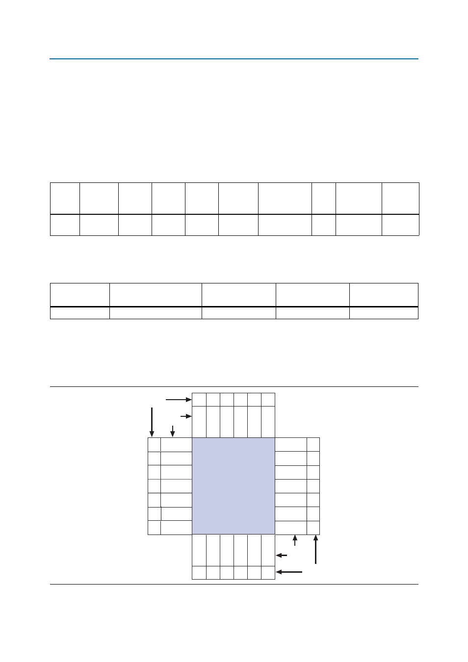
I/O Resources
shows the bank organization and I/O count for the EP4SGX230K device in
a 1517-pin FBGA package.
Table 2–2. Stratix IV GX Device EP4SGX230KF40 Features
ALMs
Equivalent
LEs
M9K
RAM
Blocks
M144K
Blocks
Total
RAM
bits
DSP
Blocks
18-bit × 18-bit
Multipliers
PLLs
Maximum
User I/O pins
Package
Type
91,200
228,000
1,235
22
17,133
161
1,288
8
736
1517-pin
FBGA
Table 2–3. Stratix IV GX Device Component Reference and Manufacturing Information
Board Reference
Description
Manufacturer
Manufacturing
Part Number
Manufacturer
Website
U33
Stratix IV GX
Altera
Corporation
EP4SGX230KF40
Figure 2–2. Stratix IV GX Device I/O Bank Diagram
Bank 8A
40
Bank 8B
24
Bank 8C
32
Bank 7C
32
Bank 6A
48
Bank 6C
EP4SGX230
Bank
Name
Number
of I/Os
40
Bank 5C
40
Bank 5A
Bank 1A
Bank 1C
Bank 2C
Bank 2A
48
48
40
40
48
Bank 7B
24
Bank 7A
40
Bank
Name
Number
of I/Os
Bank 3A
40
Bank 3B
24
Bank 3C
32
Bank 4C
32
Bank 4B
24
Bank 4A
40
4*
4*
Bank
GXBL2
4*
Bank
GXBL1
Bank
GXBL0
4*
4*
4*
Bank
GXBR2
Bank
GXBR1
Bank
GXBR0
*Number of
Transceiver
Channel