Transceiver channels, Transceiver channels –24 – Altera Transceiver Signal Integrity Development Kit, Stratix IV GX Edition User Manual
Page 34
2–24
Chapter 2: Board Components
Components and Interfaces
Transceiver Signal Integrity Development Kit,
November 2011
Altera Corporation
Stratix IV GX Edition Reference Manual
lists the SGMII and RGMII interface pin connection to the FPGA for the
Ethernet PHY device.
Transceiver Channels
The Stratix IV GX in the 1517-pin FBGA package incorporates six transceiver blocks
(GXB0 left/right, GXB1 left/right, and GXB2 left/right), with up to six transmit and
six receive channels per GXB block. For evaluation of these channels, this board offers
a total of 16 transceiver channels of the three left GXB blocks to SMA connectors.
lists the SMA connector information.
In the left GXB0 block, one transmit and one receive channel are sent to SMA
connectors J30, J32, J34 and J36. In the left GXB1 block, all six transmit and six receive
channels are sent to SMA connectors J38–J61. In the left GXB2 block, one transmit and
one receive channel are sent to SMA connectors J31, J33, J35 and J37.
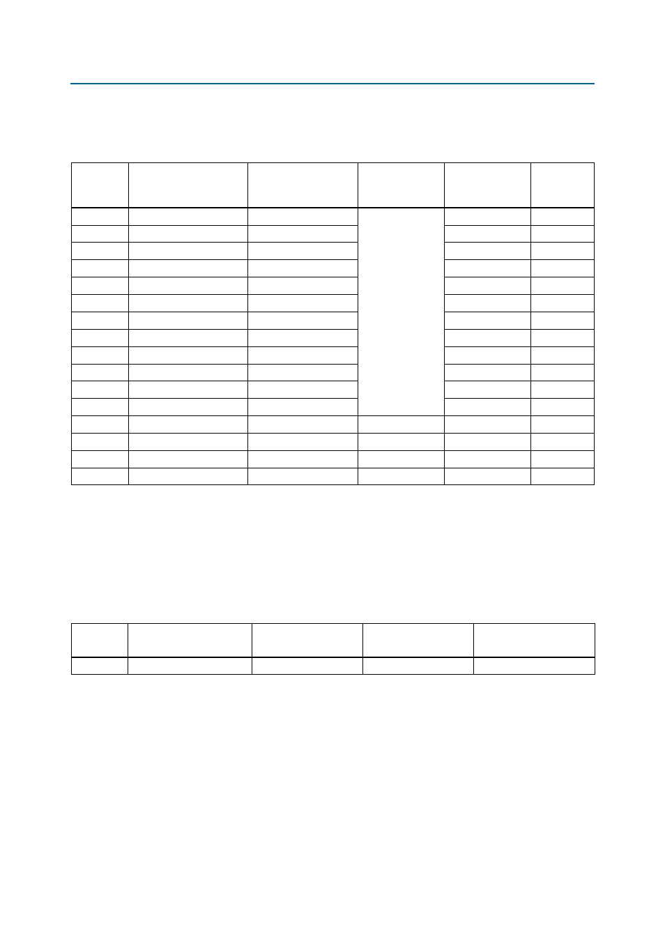
Table 2–26. Power Measurement Pin-Out
Board
Reference
Description
Schematic Signal
Name
I/O Standard
Stratix IV GX
Device Pin
Number
Other
Connections
U40 pin 11
RGMII Transmit Data 0
TXD0
2.5-V CMOS
U33 pin C29
—
U40 pin 12
RGMII Transmit Data 1
TXD1
U33 pin C30
—
U40 pin 14
RGMII Transmit Data 2
TXD2
U33 pin A27
—
U40 pin 16
RGMII Transmit Data 3
TXD3
U33 pin A29
—
U40 pin 9
RGMII Transmitter Enable
TXEN
U33 pin A31
—
U40 pin 8
RGMII Transmit Clock
GTXCLK
U33 pin B29
—
U40 pin 95
RGMII Receive Data 0
RXD0
U33 pin F27
—
U40 pin 92
RGMII Receive Data 1
RXD1
U33 pin F26
—
U40 pin 93
RGMII Receive Data 2
RXD2
U33 pin E29
—
U40 pin 91
RGMII Receive Data 3
RXD3
U33 pin E28
—
U40 pin 94
RGMII Receive Data Valid
RXDV
U33 pin D28
—
U40 pin 2
Receive Clock
RXCLK
U33 pin D29
—
U40 pin 82
SGMII Transmit Data P
ENET_SGMII_TX_P
LVDS output
U33 pin L29
—
U40 pin 81
SGMII Transmit Data N
ENET_SGMII_TX_N
LVDS output
U33 pin K29
—
U40 pin 77
SGMII Receive Data P
ENET_SGMII_RX_P
LVDS input
U33 pin D31
—
U40 pin 75
SGMII Receive Data N
ENET_SGMII_RX_N
LVDS input
U33 pin C31
—
Table 2–27. SMA Connector Component References
Board
Reference
Description
Manufacturer
Manufacturing
Part Number
Manufacturer
Website
J30–J61
SMA connector
Lighthorse Technology
LTI-SASF546-P26-X1